




These handwritten notes build Signals and Semiconductor Devices from the ground up, and this pairing feeds directly into some of the most reliably tested ideas in GATE EC.
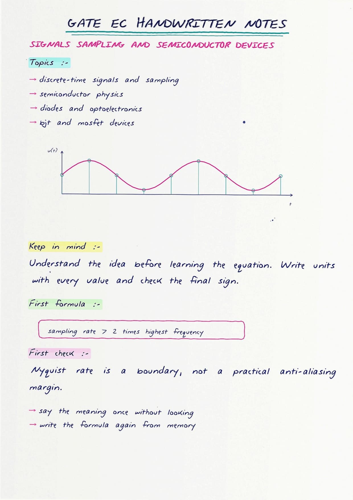
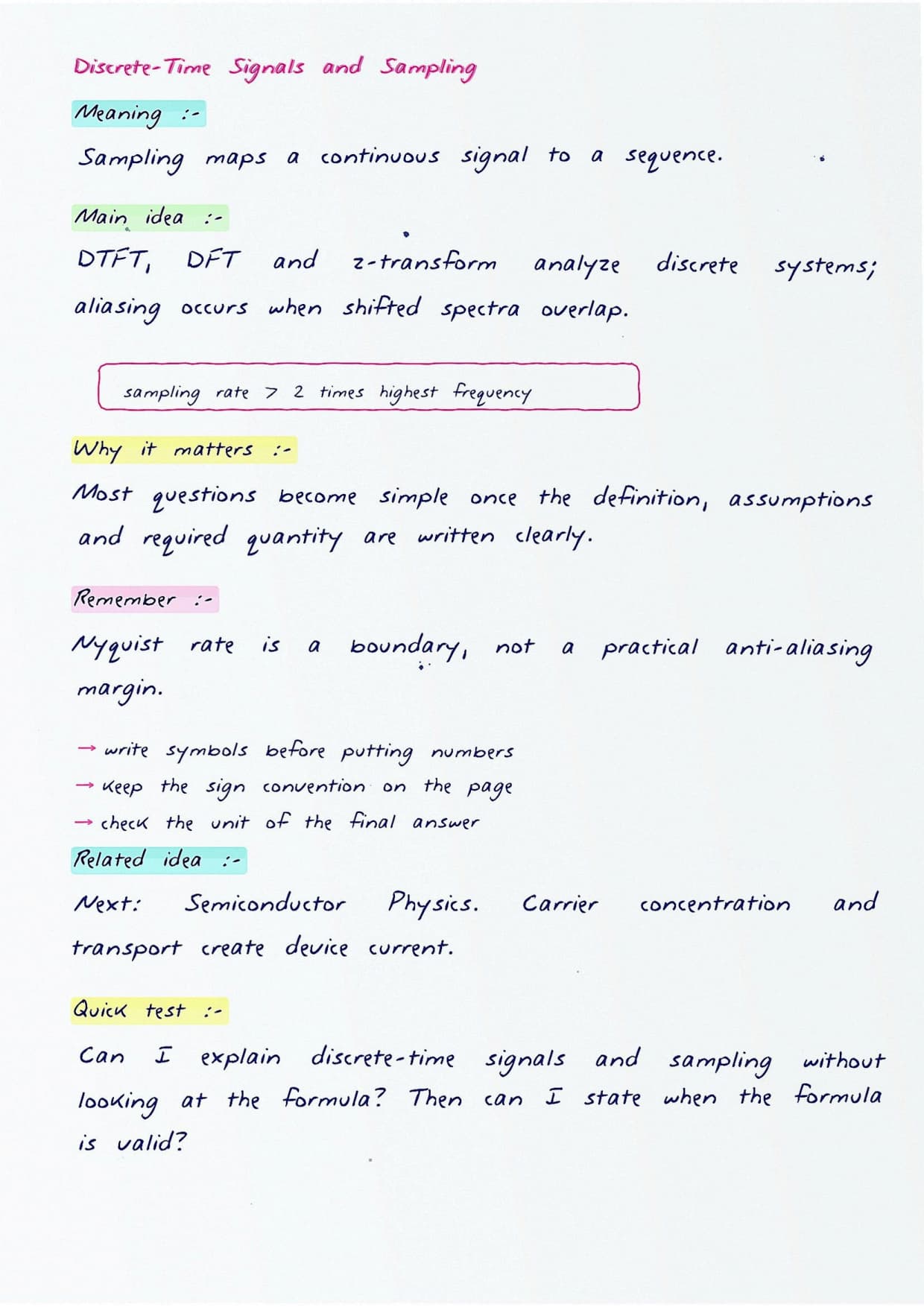
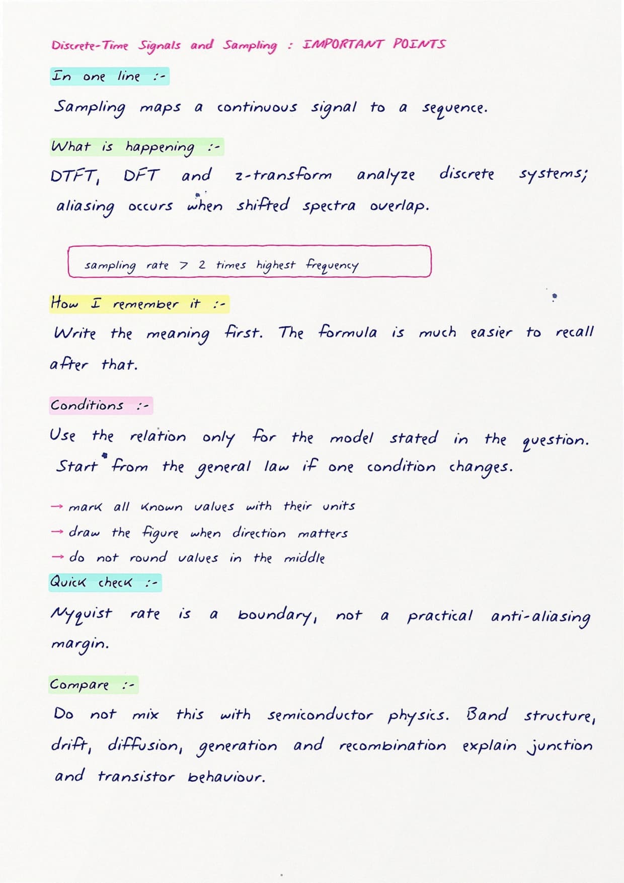
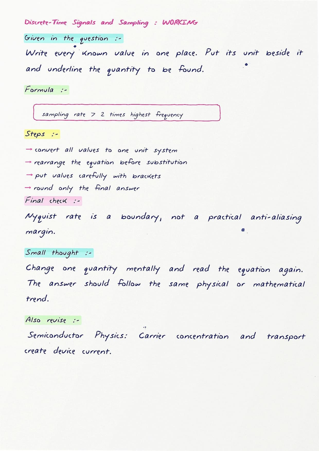
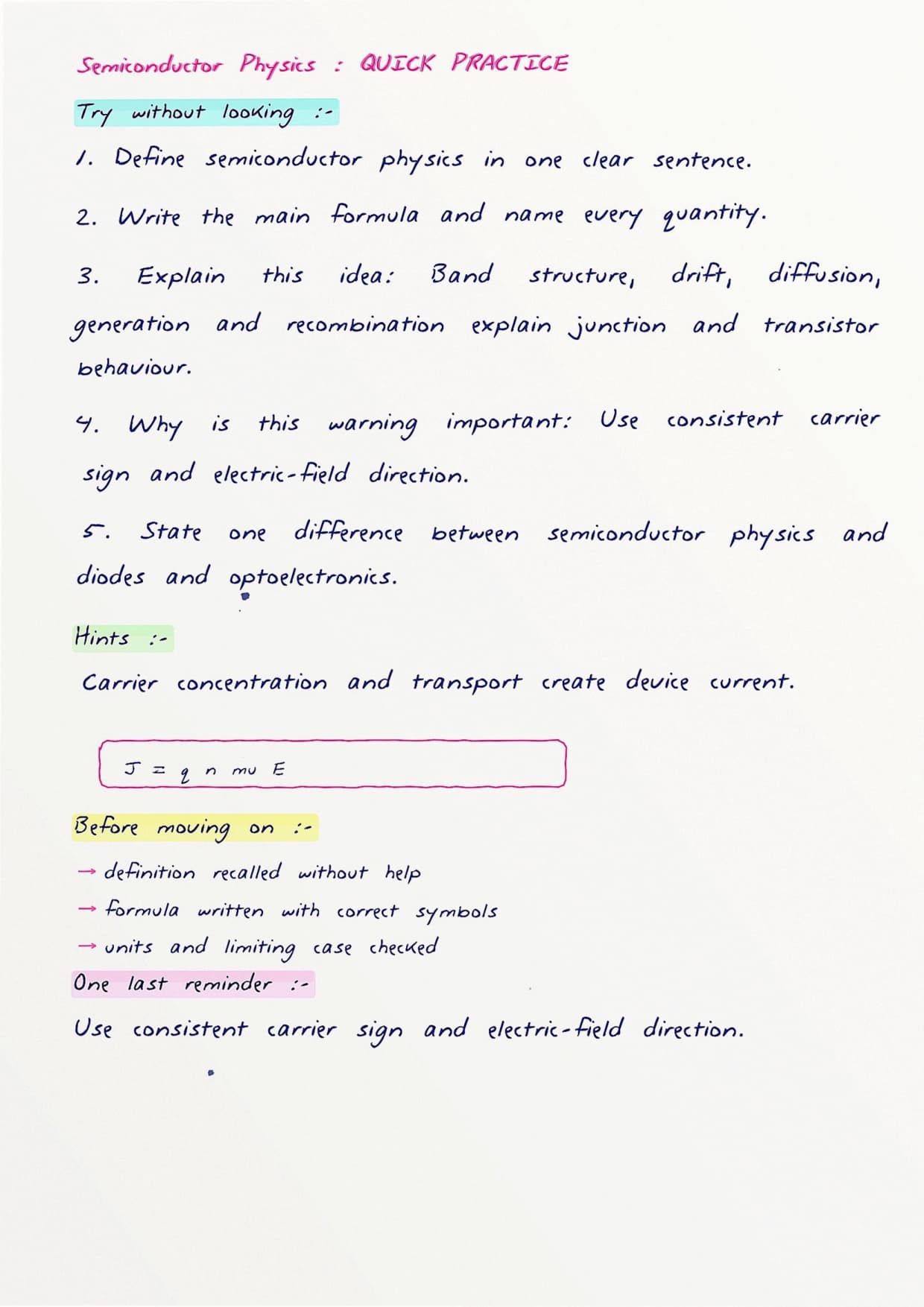
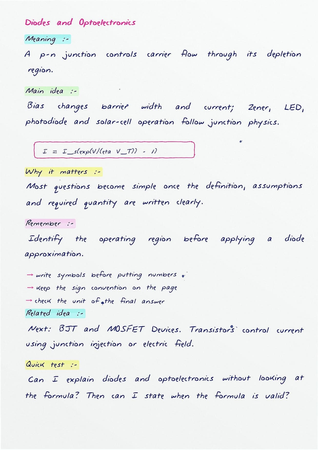
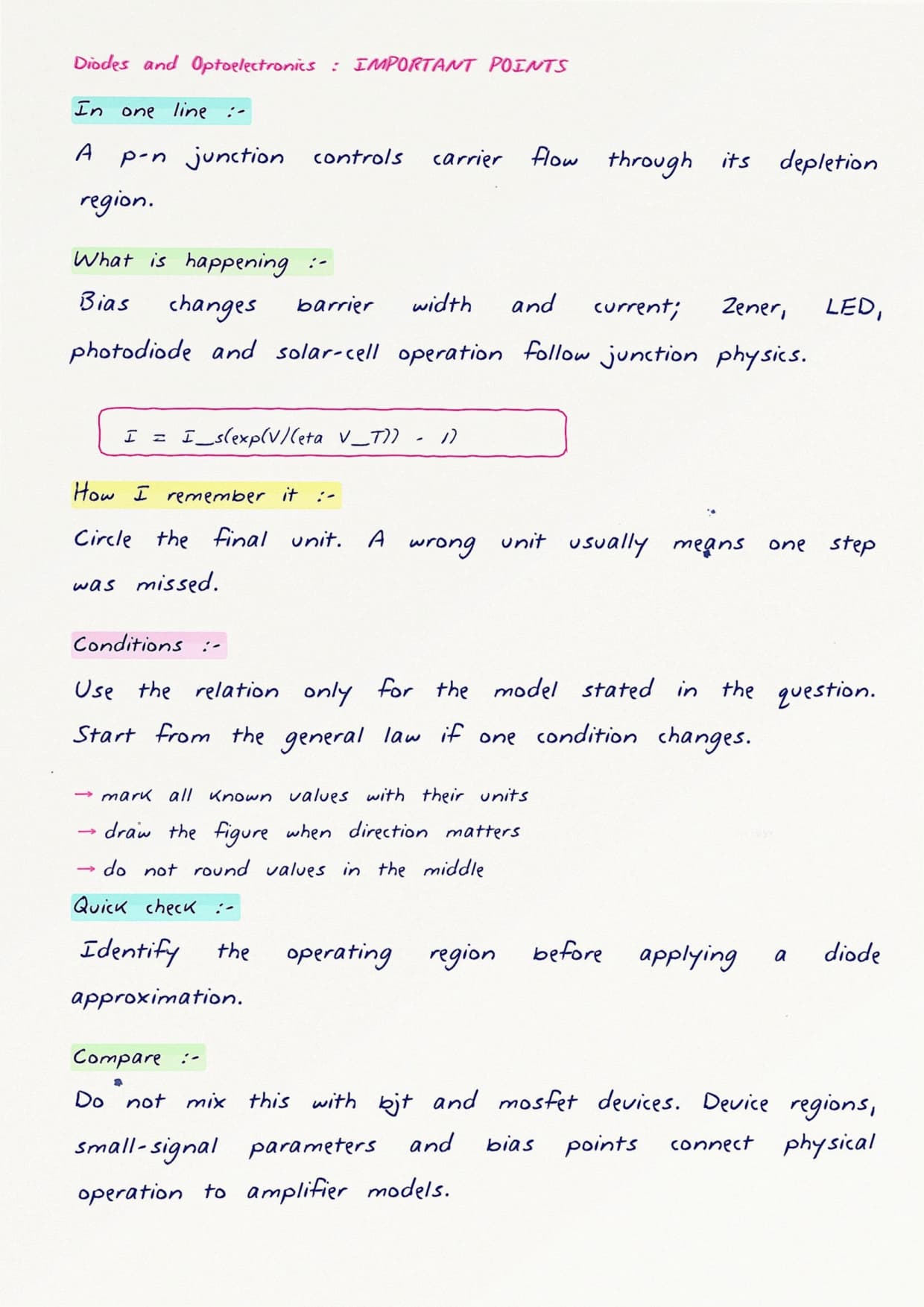
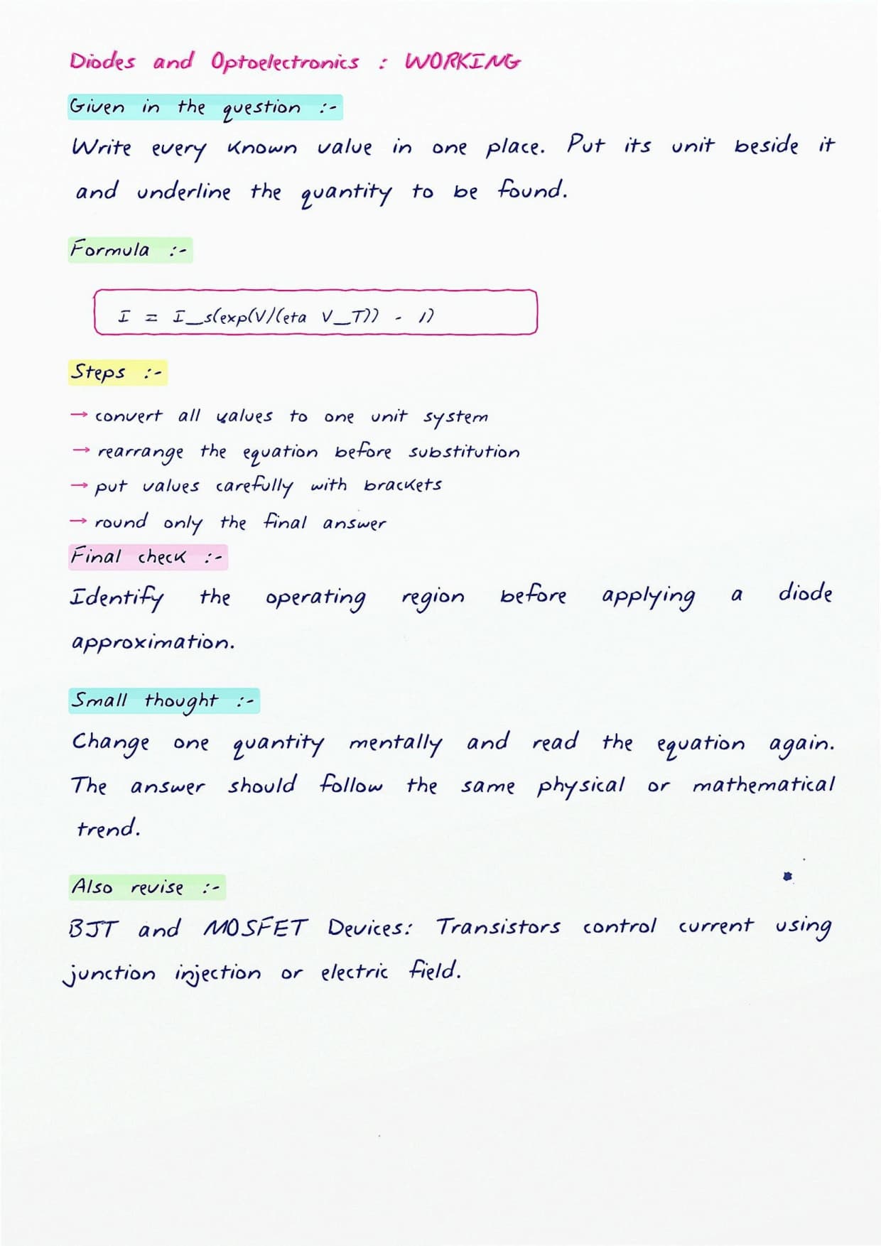
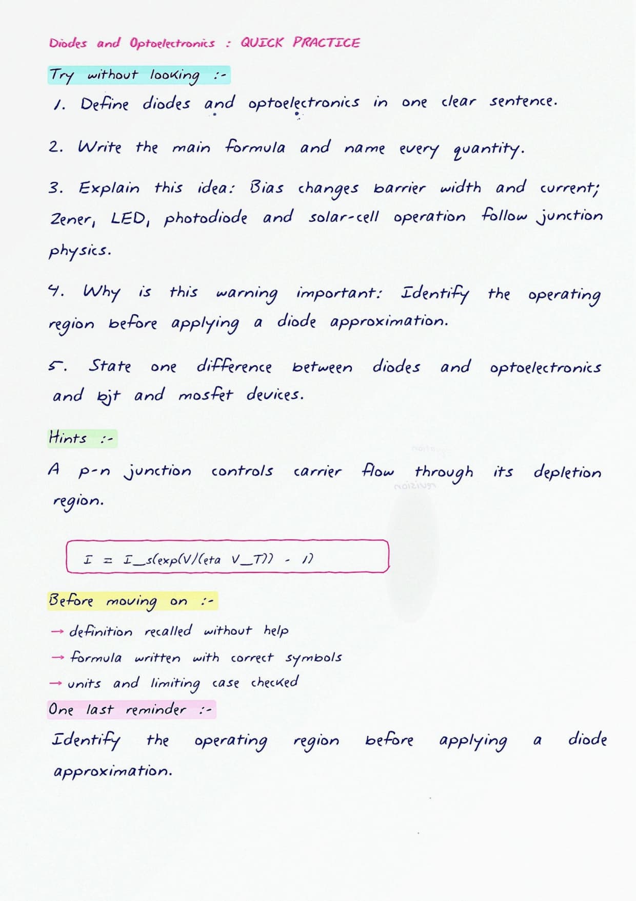
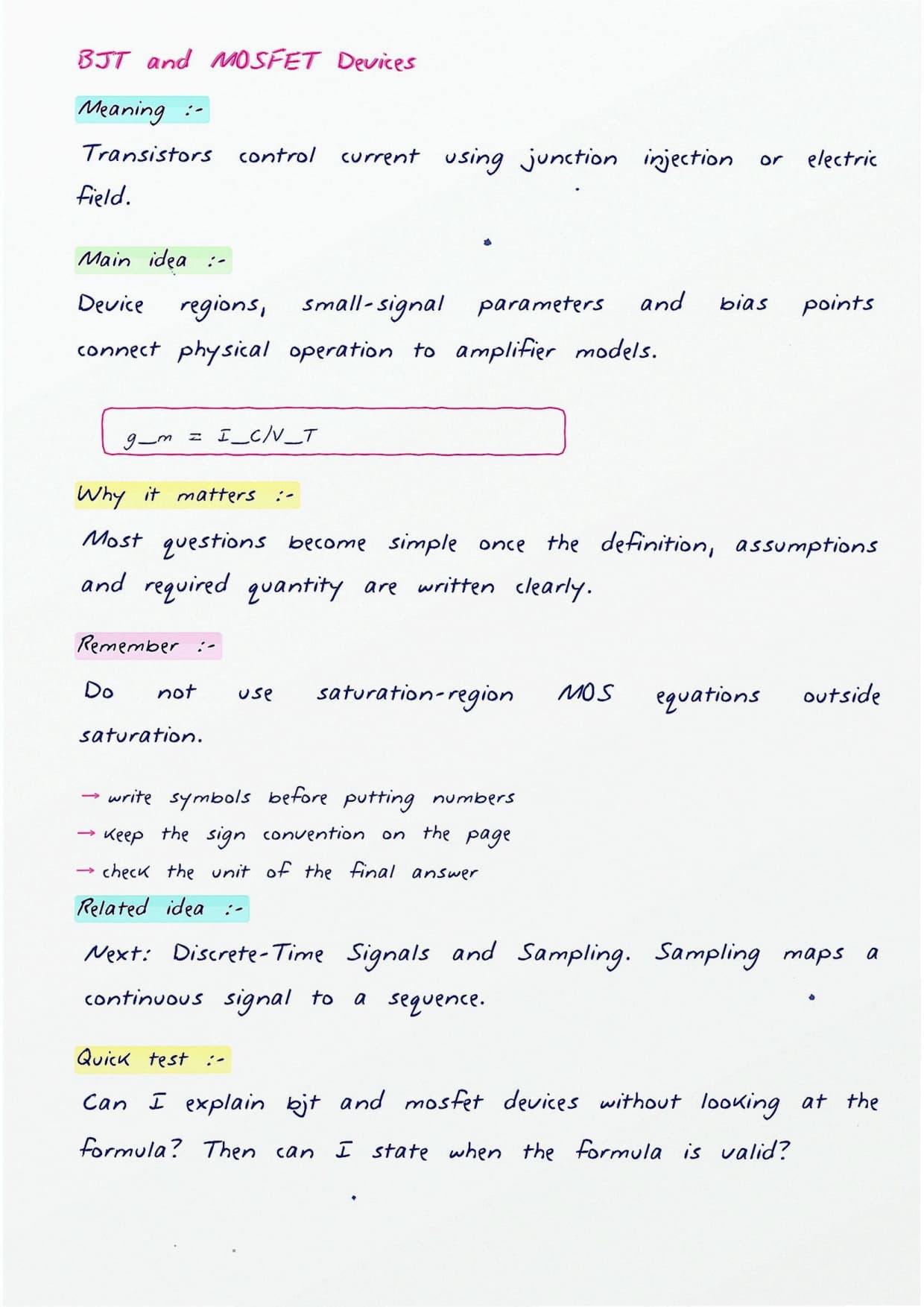
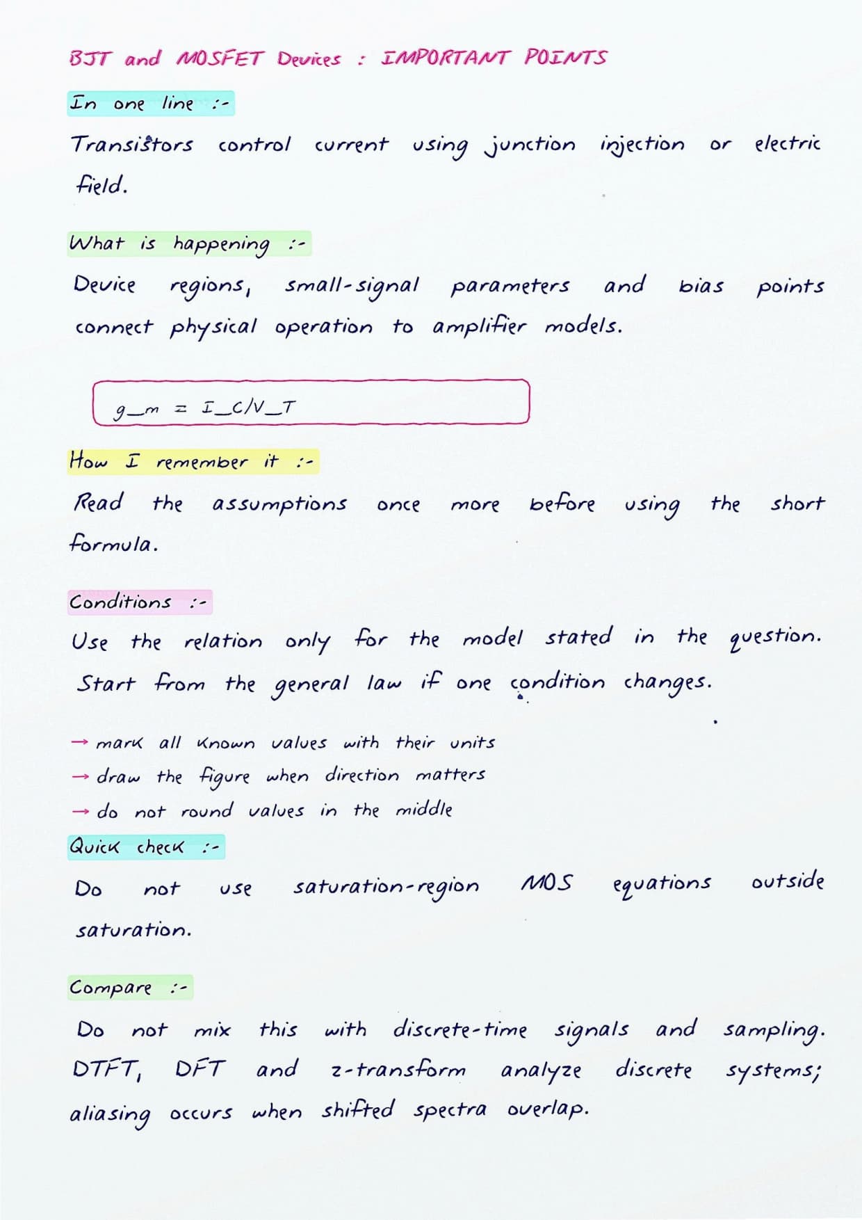
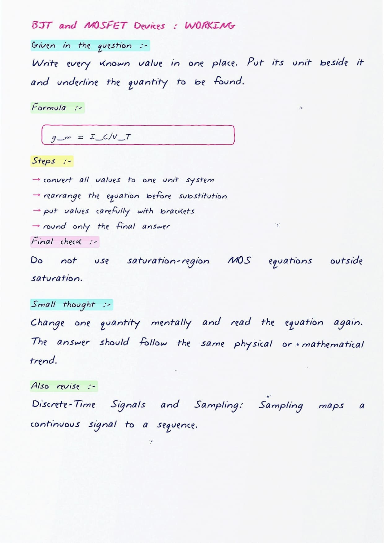
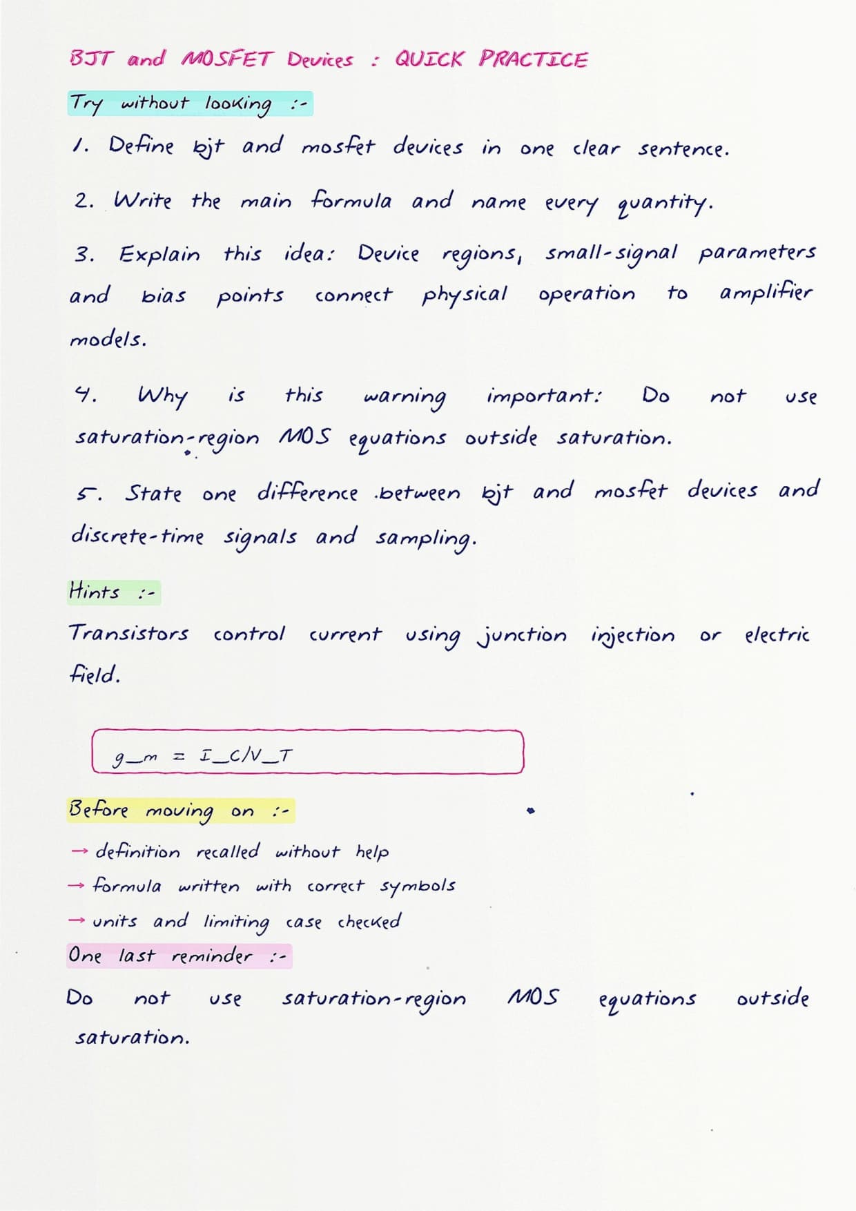
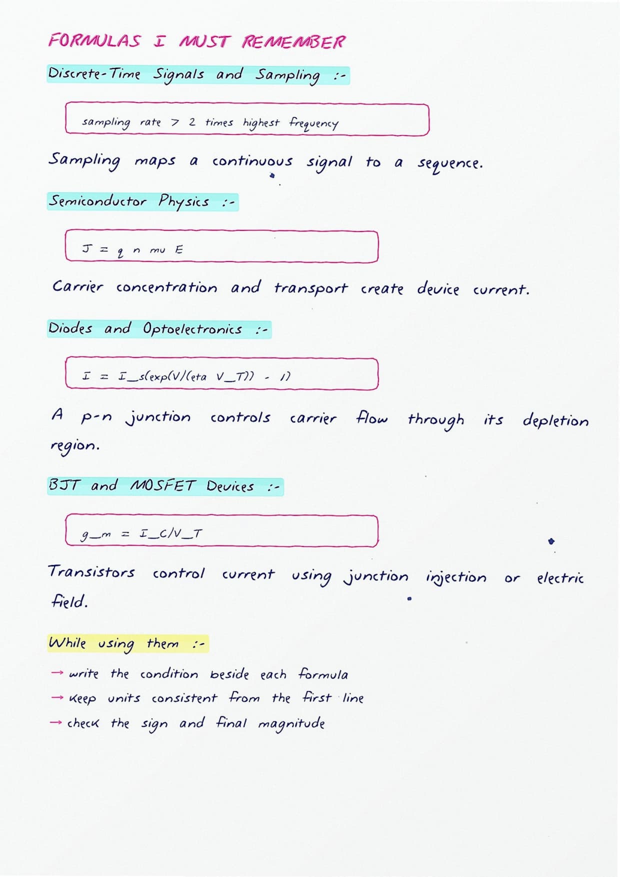
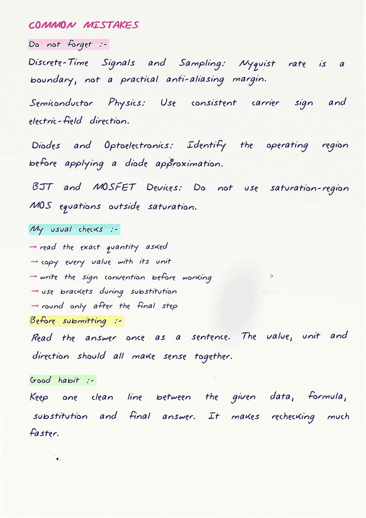
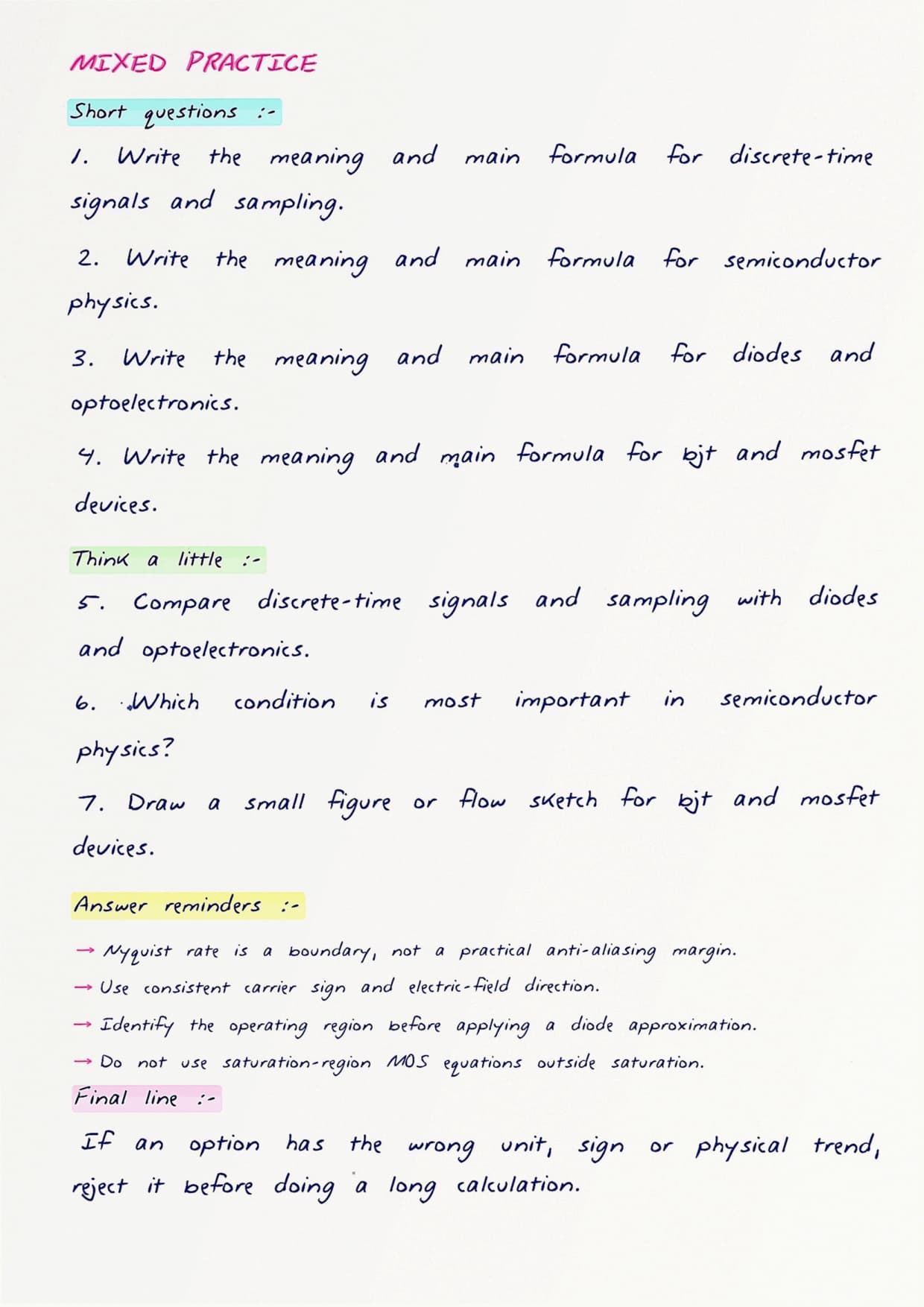
The order is deliberate. Device physics comes first, then how continuous signals become sampled data, so every later result rests on something students already understand.
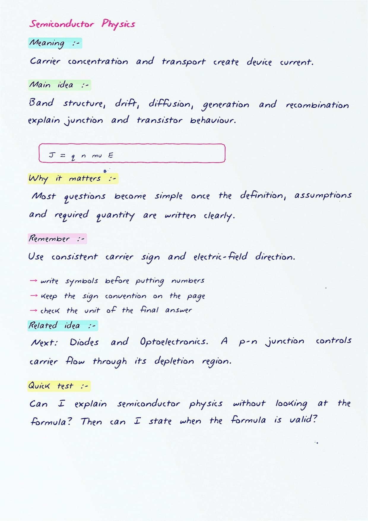
Why Start With the Physics of the Device
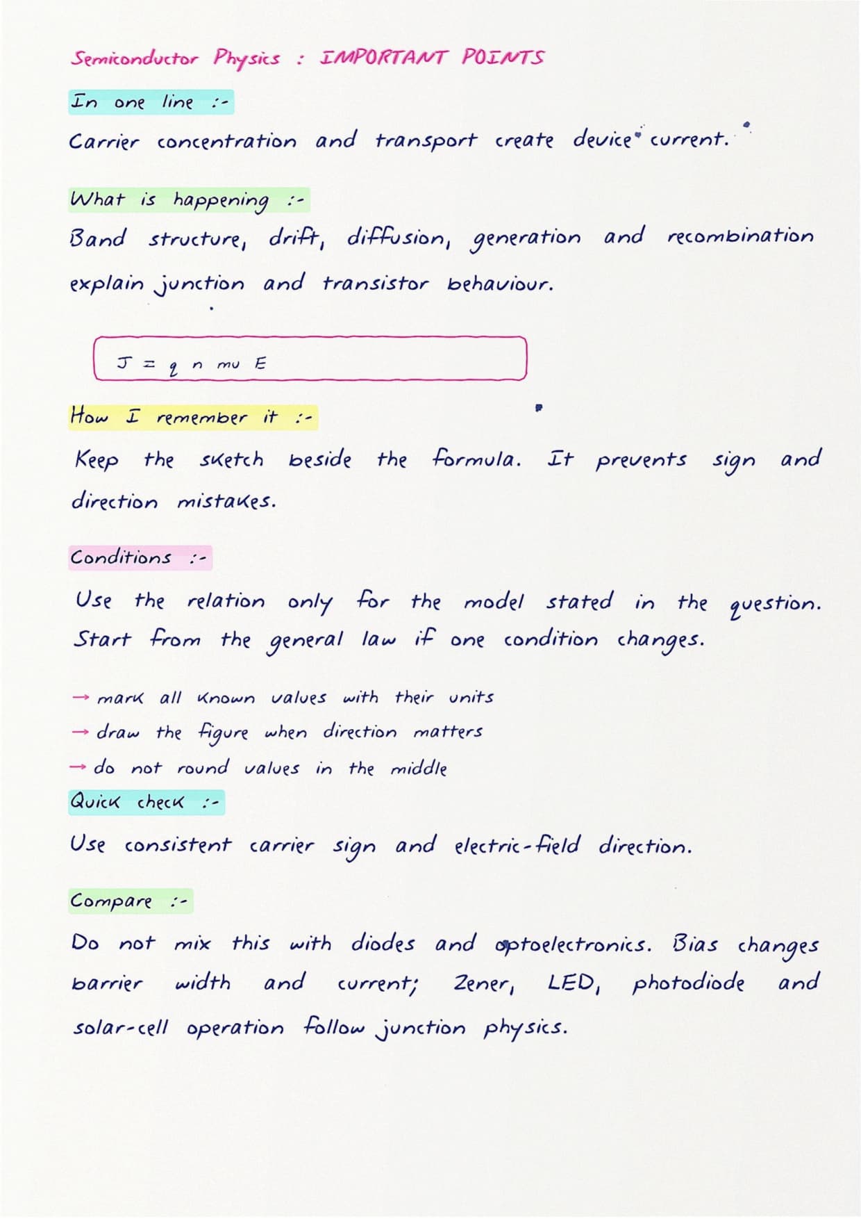
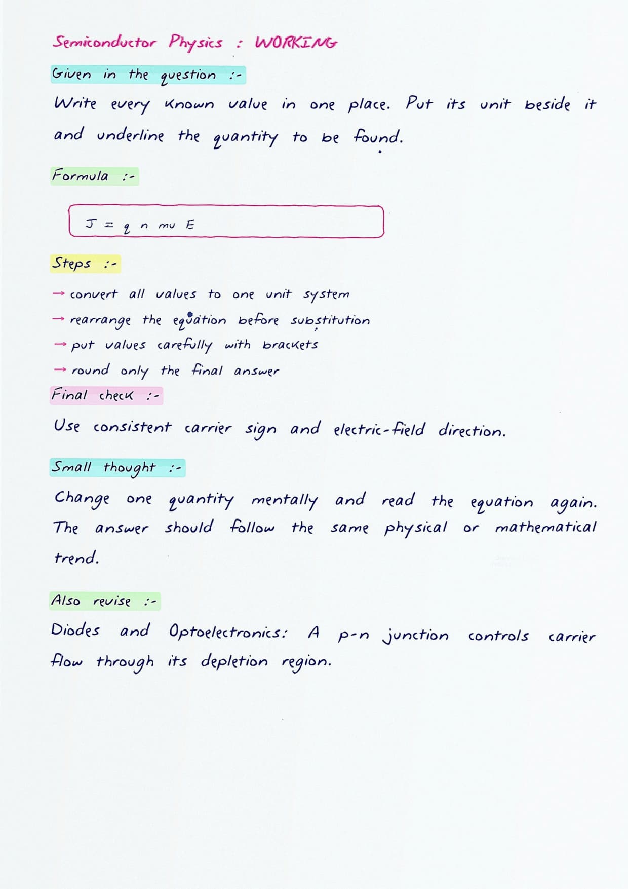
Skipping the physics is the usual reason semiconductor questions feel random. These notes anchor everything in carrier behaviour before any formula appears.
- Energy bands and what makes a material a semiconductor
- Doping and how it sets electron and hole populations
- Drift and diffusion as the two ways current actually flows
- The PN junction and why a depletion region forms
Building Up Semiconductor Behaviour Step by Step
Once the junction is clear, the notes layer devices on top of it. Each new device is shown as a small extension of the one before, so nothing feels disconnected.
- The diode current equation read in plain terms
- Capacitance effects under forward and reverse bias
- BJT action explained through carrier flow across regions
- MOS structure and how a channel forms with gate voltage
From Continuous Signals to Sampled Data
The signals half links straight to devices, because real systems capture analog signals and convert them. The notes make the transition feel natural rather than abstract.
Students see a smooth waveform, then the same waveform picked off at regular instants. That single picture is what makes the sampling theorem click.
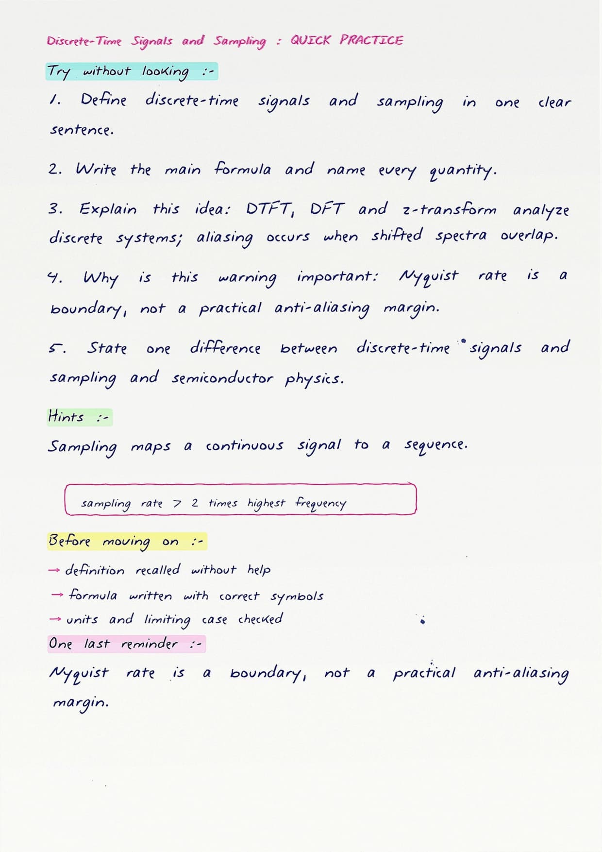
- The sampling theorem and the Nyquist rate stated simply
- Aliasing shown as overlap when sampling is too slow
- Reconstruction and why a low-pass filter recovers the signal
See Sampling Explained on the Board
Source: Kreatryx GATE - EE, ECE & IN by Unacademy
The Maths You Need Ready Before You Begin
A little groundwork makes these pages far smoother. Students who keep these tools handy rarely get stuck mid-problem.
- Comfort with exponentials and logarithms for carrier equations
- Basic Fourier intuition for what frequency content means
- Reading a frequency spectrum and spotting overlap
High-Return Ideas Worth Memorising
Some results appear so often they are worth locking in early. The notes mark each one clearly.
- The Nyquist condition and the meaning of the folding frequency
- How doping shifts the Fermi level
- The difference between drift and diffusion current
- When a MOS device enters inversion
At a Glance: Formulas and Facts to Keep Handy
The final pages act as a quick reference for the night before the exam. Students can scan them in minutes.
- Key junction and carrier relations gathered in one place
- The Nyquist rate rule for any given signal bandwidth
- Standard bias and region conditions for common devices
Signals and Semiconductor Devices Notes FAQs
Ques. Why do these notes cover signals and semiconductors together?
Ans. Because real electronic systems capture analog signals and convert them using semiconductor devices, so learning the two side by side shows how they connect in practice.
Ques. Do I need strong maths to follow these notes?
Ans. Only the basics. Comfort with exponentials, simple Fourier intuition, and reading a frequency spectrum is enough to work through every page.
Ques. Is the sampling theorem important for GATE EC?
Ans. Yes, it is a frequently tested idea, and the Nyquist rate and aliasing show up regularly, so these notes give them focused attention.
Ques. Can beginners use these notes?
Ans. They are built foundations first, starting from device physics, so a motivated beginner can follow along, though some prior exposure helps with pace.



Comments