


Education Journalist | Study Abroad Lead
There is a certain class of crystalline solids whose electrical conductivity lies between that of a conductor and an insulator, known as Semiconductors. Semiconductors are used in the production of a variety of electronic devices such as diodes, transistors, and integrated circuits. Their practical application can form the foundation of major electronic systems, across various fields. Extrinsic semiconductors are a type of semiconductor where impurities are added externally.
| Table of Content |
Key Takeaways: Semiconductors, extrinsic semiconductors, transistors, integrated circuits, p type and n type semiconductor
What are Semiconductors?
[Click Here for Sample Questions]
Semiconductors are generally amorphous or crystalline solids that have the electrical conductivity value ranging in between the conductors (generally metals) and insulators (materials that can’t conduct electricity). This means that semiconductors do conduct current, but only partly.

Semiconductors can be further divided into two types :
- Intrinsic Semiconductors
- Extrinsic Semiconductors
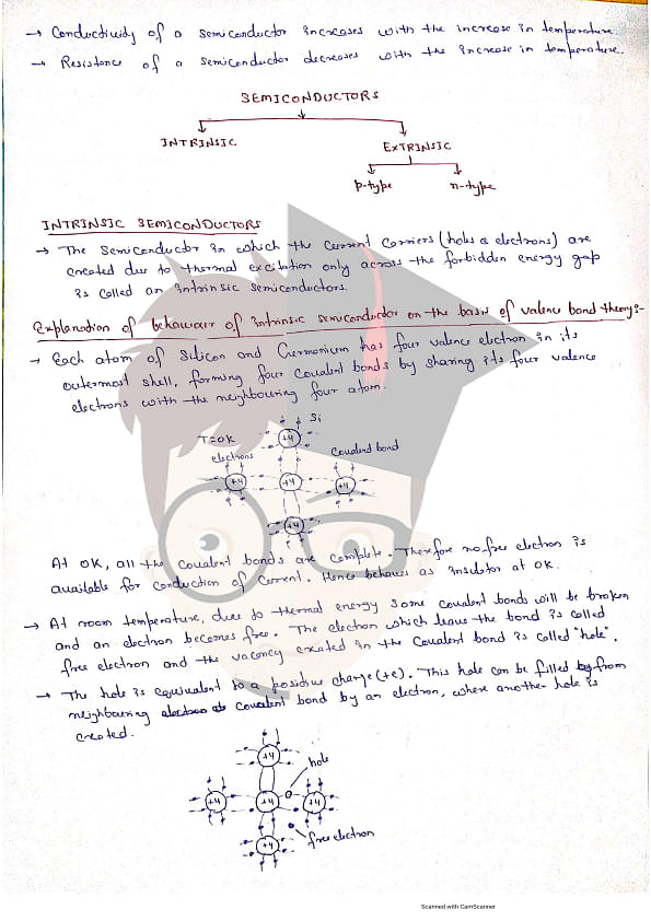
Intrinsic Semiconductors
Intrinsic Semiconductors are those which conduct electricity when the temperature is raised above room temperature. Since outside temperature can change the conductivity, the device that incorporates the mechanism of intrinsic semiconductors can pose serious problems.
Due to this reason, scientists, after significant research and experimentation, came up with the concept of extrinsic semiconductors.
The video below explains this:
Semiconductors and Insulators Detailed Video Explanation:
Also Read:
| Related Articles | ||
|---|---|---|
| Junction Transistor | Digital Electronics and Logic Gates | Rectifier |
| Zener Diode | Bridge Rectifier | Application of Junction Diode |
Extrinsic Semiconductors
[Click Here for Sample Questions]
Extrinsic semiconductors are those in which impurity is specifically added from the outside. The impurities are generally in the form of either trivalent or pentavalent atoms. Ambient temperature doesn’t play any role in terms of electrical conductivity. It is the impurity that determines the value of conductivity. The impurities are known as dopants while the process is known as doping. This results in Extrinsic Semiconductors also being known as Doped Semiconductors.

Semiconductor Electronics Class 12 Important Notes PDF
Semiconductor Electronics Class 12 Important Notes


Types of Extrinsic Semiconductors
[Click Here for Sample Questions]
Extrinsic semiconductors are further divided into two types which are:
- N-type Semiconductors
- P-type Semiconductors
N-type Semiconductor
[Click Here for Sample Questions]
When the dopants from group V of the periodic table are added to the semiconductor, it leads to the formation of an N-type semiconductor.

Let’s say a pentavalent atom Arsenic (As) is added to the semiconductor which has 5 electrons in its valence shell. Four of the electrons of As will bond with the neighboring Ge atom while the remaining one electron will move freely in the semiconductor thus the ionization enthalpy which is needed to free the remaining electron of Arsenic will decrease.
The concept of N-type Semiconductor can be understood by looking at the image given below:

Figure a, represents the free electron of the pentavalent atom which tends to move freely in the semiconductor. While figure b indicates a graphical representation of the various energy bands and position of the donor level
It is seen that the donor level is below the conduction band but it is near to it. Due to this, the remaining electron of the Arsenic can easily jump into the conduction band because of the low energy difference between the two.
What does the term donor level signify?
It has been stated that there is one extra electron of Arsenic that isn’t able to form any bond in the lattice structure, due to which the semiconductor has an extra electron. This is the reason why the term donor is used here.
In n-type semiconductors, the number of electrons (ne) will be more than the number of holes (nh).
P-type Semiconductor
[Click Here for Sample Questions]
When the impurities in the form of trivalent atoms like Aluminium are added to the semiconductor, then it leads to the formation of a P-type Semiconductor.

On adding the trivalent Aluminium atom that has three electrons in its valence shell, all of them will form a bond with the Ge atom but one extra electron is still needed to complete the pairing of four electrons of the Ge atom. Aluminium has just three valence electrons which lead to the formation of the hole between Al and Ge.
To fill up this gap, the electron from outer orbit will be shifted to this hole but in turn, it forms a gap at its original location.
The above-mentioned text can be easily understood by looking at the image given below:

Figure a represents the formation of a hole that is formed due to the trivalent impurity atom. While figure b indicates the graphical representation of various energy bands and an acceptor level. It can be observed that the acceptor level lies just above the valence band and it is nearby to it. It means that the electrons can easily jump from the valence band to the acceptor level and the majority of the acceptor atoms can be ionized at room temperature.
What does the term acceptor level signify?
It is a well-known fact that the number of holes (positive charge) is more than the number of electrons. Due to this reason, it can exhibit the property of the acceptor.
In p-type semiconductors, the number of holes (nh) will always be more than the number of electrons (ne).
Things to Remember
- Semiconductors generally consist of atoms like Germanium (Ge) or Silicon (Se). But once impurity is added to the semiconductor without disrupting the structure lattice, then the same semiconductor will be termed as the extrinsic semiconductor.
- The impurity added to the semiconductor is called dopant and the process of doing the same is called doping.
- The ambient temperature doesn’t play any role in the electrical conductivity. Rather, it is the impurity that determines the electrical conductivity.
- The impurities added to the semiconductor should be either from group III or V of the periodic table as the atomic size of the atoms of group III, IV, and V are approximately equal to each other. Thus, either pentavalent or trivalent impurities are added to the semiconductor.
- There will be two types of charge carriers depending on the kind of impurity added to the semiconductor which are:
- Majority charge carriers
- Minority charge carriers
- There are two types of Extrinsic semiconductors:
- N-type Semiconductor
- P-type Semiconductor
Also Read:
Sample Questions
Ques: What is an Extrinsic Semiconductor? (2 marks)
Ans: Extrinsic semiconductors are those in which impurity is specifically added from the outside. The impurities are generally in the form of either trivalent or pentavalent atoms. Ambient temperature doesn’t play any role in terms of electrical conductivity. It is the impurity that determines the value of conductivity. The impurities are known as dopants while the process is known as doping. This results in Extrinsic Semiconductors also being known as Doped Semiconductors.
Ques: Name some pentavalent and trivalent atoms that serve as the dopants. (2 marks)
Ans: Dopant refers to the impurity that is deliberately added to a semiconductor to modify its conductivity.
Pentavalent atoms in the case of N-type Semiconductors are Arsenic (As), Phosphorous (P), and Antimony (Sb). The charge carriers are electrons, which are negatively charged particles. They are called donor atoms.
The trivalent atoms for p-type semiconductors are Boron (B), Aluminium (Al) and Gallium (Ga). They create a positively charged site and are known as acceptor atoms.
Ques: What happens to the width of depletion layer of a p-n junction when it is (a) forward biased, (b) reverse biased? (Delhi 2011) (2 marks)
Ans. The Depletion layer is a region in a P-N junction diode where mobile charge carriers are absent. The Depletion layer acts like a barrier that opposes the flow of electrons from n-side and holes from p-side.The width of the depletion layer changes under certain circumstances.
- The width of the depletion layer of the p-n junction decreases when forward biased.
- The width of the depletion layer of the p-n junction increases when reverse biased.
Ques: Specify the majority and minority charge carriers in both the types of Extrinsic Semiconductors. (3 marks)
Ans: Charge carriers present in large quantities are called majority charge carriers. They carry the majority of the electric charge/current in the semiconductor, hence the name. Majority charge carriers are primarily responsible for the flow of the electric current.
Charge carriers present in small quantities are called minority charge carriers. They carry a minor amount of electric charge/current in the semiconductor.
For N-type Semiconductors, the majority charge carriers are electrons while the minority charge carriers are holes.
For P-type semiconductors, the majority charge carriers are holes while the minority charge carriers are the electrons.
Ques: What is the difference between an extrinsic and intrinsic conductor? (4 marks)
Ans. The difference between an intrinsic and extrinsic semiconductor is:
| Intrinsic Semiconductor | Extrinsic Semiconductor |
|---|---|
| Pure semiconductor | Impure semiconductor |
| Electron and holes have equal density | Electron and Holes have unequal density |
| Low electrical conductivity | High electrical conductivity |
| Only dependent on temperature | Dependent on temperature as well as on the amount of impurity |
| Small band gap between conduction (C.B) and valence band (V.B). | Large band gap between conduction (C.B) and valence band (V.B). |
| Examples: Si, Ge | Examples: Ga, As, P |
Ques: Indicate the donor and acceptor levels on an energy band diagram for an extrinsic semiconductor. (3 marks)
Ans. N-type Extrinsic Semiconductor P-type Extrinsic Semiconductor

Ques: Does ambient temperature play any role in the electrical conductivity in the case of extrinsic semiconductors? (2 marks)
Ans: It is to be noted that the electrical conductivity of the extrinsic semiconductors solely depends on the type of impurity added and not on the ambient temperature. Change in the ambient temperature can increase the randomness of already formed holes or free electrons but will never impact the conductivity.
Ques: Write the two processes that take place in the formation of a p-n junction. Explain with the help of a diagram, the formation of depletion region and barrier potential in a p-n junction. (Delhi, ‘17) (3 marks)
Ans. Diffusion and Drift are two important processes involved during the formation of a p-n junction.

Formation of depletion region and barrier potential: At the instant of p-n junction formation, the free electrons near the junction diffuse across the junction into the p region and combine with holes. Thus, on combining with the hole, it makes a negative ion and leaves a positive ion on the n-side. The depletion layer is formed from the two layers of immobile positive and immobile negative charges.

Further, as electrons diffuse across the junction a point is reached where the negative charge repels any further diffusion of electrons. This depletion region now acts as a barrier. Now the external energy is supplied to get the electrons to move across the barrier of the electric field. The potential difference required to move the electrons through the electric field is called barrier potential.
Ques. Which of the substances is preferred in semiconductor devices and why? Silicon or Germanium? (2 marks)
Ans. Silicon is preferred instead of Germanium in semiconductor devices. It is so because:
- Silicon has fewer number of free electrons because of which its collector cut-off current is smaller than Germanium.
- A Germanium Diode has a lower peak inverse voltage than a Silicon Diode.
- Silicon is more economically feasible than Germanium.
For Latest Updates on Upcoming Board Exams, Click Here: https://t.me/class_10_12_board_updates
Check-Out:


Comments