
CBSE Class 12 Physics Question Paper 2024 PDF (Set 2- 55/4/2) is available for download here. CBSE conducted the Physics exam on March 4, 2024 from 10:30 AM to 1:30 PM. The total marks for the theory paper are 70. The question paper contains 20% MCQ-based questions, 40% competency-based questions, and 40% short and long answer type questions.
CBSE Class 12 Physics Question Paper 2024 (Set 2- 55/4/2) with Answer Key
| CBSE Class 12 2024 Physics Question Paper with Answer Key | Check Solution |
CBSE Class 12 2024 Physics Questions with Solutions
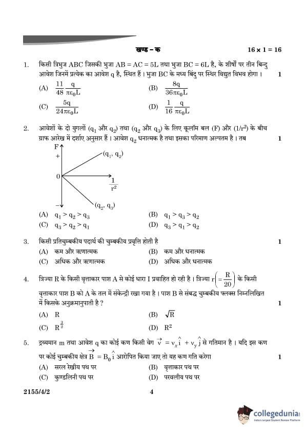
Three point charges, each of charge \( q \), are placed on vertices of a triangle \( ABC \), with \( AB = AC = 5L \), \( BC = 6L \). The electrostatic potential at the midpoint of side \( BC \) will be:
View Solution
Electrostatic Potential at the Midpoint of \( BC \)
Step 1: Formula for Electrostatic Potential
- The electrostatic potential at a point due to a charge \( q \) at distance \( r \) is:
\[ V = \frac{1}{4\pi \epsilon_0} \frac{q}{r} \]
Step 2: Contribution of Charges at \( B \) and \( C \)
- The midpoint of \( BC \) is equidistant from charges at \( B \) and \( C \).
- Distance of midpoint from \( B \) or \( C \):
\[ r_{B} = r_C = \frac{BC}{2} = \frac{6L}{2} = 3L \]
- Potential due to charge at \( B \):
\[ V_B = \frac{1}{4\pi \epsilon_0} \frac{q}{3L} \]
- Potential due to charge at \( C \):
\[ V_C = \frac{1}{4\pi \epsilon_0} \frac{q}{3L} \]
- Total contribution from \( B \) and \( C \):
\[ V_{BC} = 2 \times \frac{q}{12\pi \epsilon_0 L} = \frac{2q}{12\pi \epsilon_0 L} = \frac{q}{6\pi \epsilon_0 L} \]
Step 3: Contribution of Charge at \( A \)
- Distance from \( A \) to the midpoint of \( BC \) (Using Apollonius theorem):
\[ r_A = \sqrt{(5L)^2 - (3L)^2} = \sqrt{25L^2 - 9L^2} = \sqrt{16L^2} = 4L \]
- Potential due to charge at \( A \):
\[ V_A = \frac{1}{4\pi \epsilon_0} \frac{q}{4L} = \frac{q}{16\pi \epsilon_0 L} \]
Step 4: Total Electrostatic Potential at Midpoint \[ V = V_{BC} + V_A \]
\[ V = \frac{q}{6\pi \epsilon_0 L} + \frac{q}{16\pi \epsilon_0 L} \]
\[ V = \frac{16q + 6q}{96\pi \epsilon_0 L} \]
\[ V = \frac{22q}{96\pi \epsilon_0 L} = \frac{11q}{48\pi \epsilon_0 L} \]
Thus, the electrostatic potential at the midpoint of \( BC \) is:
\[ \frac{11q}{48\pi \epsilon_0 L} \]
which matches option (A).
Quick Tip: The electrostatic potential at a point due to multiple charges is the algebraic sum of the potentials due to individual charges.
The Coulomb force (\( F \)) versus \( \frac{1}{r^2} \) graphs for two pairs of point charges (\( q_1 \) and \( q_2 \)) and (\( q_2 \) and \( q_3 \)) are shown in the figure. The charge \( q_2 \) is positive and has the least magnitude. Then:
View Solution
Understanding Coulomb Force Variation
- According to Coulomb’s Law, the force between two charges is:
\[ F = \frac{1}{4\pi \epsilon_0} \frac{|q_1 q_2|}{r^2} \]
- The slope of the \( F \) vs. \( \frac{1}{r^2} \) graph represents \( |q_1 q_2| \).
- Since \( q_2 \) has the least magnitude and is positive, comparing slopes gives:
\[ q_3 > q_1 > q_2 \]
Thus, the correct order is \( q_3 > q_1 > q_2 \), matching option (D).
Quick Tip: A steeper slope in the \( F \) vs. \( \frac{1}{r^2} \) graph means a greater product of charge magnitudes.
The magnetic susceptibility for a diamagnetic material is:
View Solution
Magnetic Susceptibility of Diamagnetic Materials
- Magnetic susceptibility (\( \chi_m \)) measures how a material responds to an external magnetic field.
- For diamagnetic materials, \( \chi_m \) is:
- Negative (they repel magnetic fields).
- Small (weak effect compared to paramagnetic or ferromagnetic materials).
\[ \chi_m \approx -10^{-5} to -10^{-6} \]
Thus, the correct answer is (A) Small and negative.
Quick Tip: Diamagnetic materials like copper, bismuth, and gold have a small negative magnetic susceptibility and oppose external magnetic fields.
A circular loop A of radius \( R \) carries a current \( I \). Another circular loop B of radius \( r = \frac{R}{20} \) is placed concentrically in the plane of A. The magnetic flux linked with loop B is proportional to:
View Solution
Magnetic Flux Linked with Loop B
Step 1: Magnetic Field at the Center of a Current-Carrying Loop
The magnetic field at the center of a circular loop carrying current \( I \) is:
\[ B = \frac{\mu_0 I}{2R} \]
where:
- \( \mu_0 \) = Permeability of free space,
- \( R \) = Radius of loop A.
Step 2: Magnetic Flux Through Loop B
The magnetic flux through loop B is given by:
\[ \Phi = B \cdot A \]
where:
- \( A \) is the area of loop B:
\[ A = \pi r^2 = \pi \left( \frac{R}{20} \right)^2 = \frac{\pi R^2}{400} \]
- Substituting \( B \) from Step 1:
\[ \Phi = \left( \frac{\mu_0 I}{2R} \right) \times \frac{\pi R^2}{400} \]
\[ \Phi = \frac{\mu_0 I \pi R^2}{800R} \]
\[ \Phi \propto R \]
Thus, the magnetic flux linked with loop B is proportional to \( R \), which matches option (A).
Quick Tip: For a concentric loop system, the magnetic flux linkage depends on both the field of the larger loop and the area of the smaller loop.
A particle of mass \( m \) and charge \( q \) is moving with velocity \( \mathbf{v} = v_x \hat{i} + v_y \hat{j} \). If it is subjected to a magnetic field \( \mathbf{B} = B_0 \hat{i} \), it will move in a:
View Solution
Motion of a Charged Particle in a Magnetic Field
- The Lorentz Force on a charged particle moving in a magnetic field is:
\[ \mathbf{F} = q (\mathbf{v} \times \mathbf{B}) \]
- Given \( \mathbf{B} = B_0 \hat{i} \) and \( \mathbf{v} = v_x \hat{i} + v_y \hat{j} \), we calculate the cross-product:
\[ \mathbf{F} = q [(v_x \hat{i} + v_y \hat{j}) \times (B_0 \hat{i})] \]
- Since \( \hat{i} \times \hat{i} = 0 \) and \( \hat{j} \times \hat{i} = -\hat{k} \), we get:
\[ \mathbf{F} = -q v_y B_0 \hat{k} \]
- The force acts perpendicular to the velocity component in the \( yz \)-plane, causing circular motion in that plane.
- The velocity component along \( x \)-direction remains unchanged, leading to a helical path.
Thus, the correct answer is (C) helical path.
Quick Tip: A charged particle moves in a helical path when its velocity has a component parallel and perpendicular to the magnetic field.
The quantum nature of light explains the observations on the photoelectric effect as:
View Solution
Explanation of Photoelectric Effect
- According to Einstein’s Photoelectric Equation:
\[ K_{\max} = h f - \phi \]
where:
- \( h \) = Planck’s constant,
- \( f \) = Frequency of incident radiation,
- \( \phi \) = Work function of the metal.
- If \( f < f_0 \) (threshold frequency), no electrons are emitted.
- This confirms the quantum nature of light, supporting option (A).
Quick Tip: In the photoelectric effect, electrons are emitted only if the photon energy exceeds the work function of the metal.
The phase difference between electric field \( \mathbf{E} \) and magnetic field \( \mathbf{B} \) in an electromagnetic wave propagating along the \( z \)-axis is:
View Solution
Phase Relationship in Electromagnetic Waves
- In an electromagnetic wave, the electric field \( \mathbf{E} \) and the magnetic field \( \mathbf{B} \) are:
1. Perpendicular to each other.
2. Perpendicular to the direction of wave propagation.
3. In phase with each other.
- The wave equations are:
\[ E = E_0 \sin(kz - \omega t) \]
\[ B = B_0 \sin(kz - \omega t) \]
- Since both fields oscillate in phase, the phase difference is \( 0 \).
Thus, the correct answer is (A) \( 0 \).
Quick Tip: In an electromagnetic wave, the electric and magnetic fields are in phase and perpendicular to each other and the direction of wave propagation.
The radius (\( r_n \)) of the \( n^{th} \) orbit in the Bohr model of the hydrogen atom varies with \( n \) as:
View Solution
Bohr’s Model and Radius of Electron Orbits
Step 1: Formula for Bohr’s Radius
According to Bohr’s Model, the radius of an electron in the \( n^{th} \) orbit of a hydrogen atom is:
\[ r_n = \frac{4\pi \epsilon_0 \hbar^2}{m e^2} n^2 \]
where:
- \( \epsilon_0 \) = Permittivity of free space,
- \( \hbar \) = Reduced Planck’s constant,
- \( m \) = Mass of the electron,
- \( e \) = Charge of the electron.
Step 2: Understanding the Proportionality
- Since all constants remain unchanged, we get:
\[ r_n \propto n^2 \]
Step 3: Conclusion
- The radius of an orbit increases quadratically with \( n \).
- Thus, the correct answer is (C) \( r_n \propto n^2 \).
Quick Tip: In Bohr’s Model, orbit radius varies as \( n^2 \), while energy varies as \( \frac{1}{n^2} \).
An AC source \( V = 282 \sin(100t) \) volt is connected across a \( 1 \mu F \) capacitor. The RMS value of current in the circuit will be (Take \( \sqrt{2} = 1.41 \)):
View Solution
RMS Current Calculation
Step 1: Given Data
- Peak voltage: \( V_0 = 282V \)
- Angular frequency: \( \omega = 100 \)
- Capacitance: \( C = 1 \mu F = 10^{-6} F \)
Step 2: Reactance of the Capacitor \[ X_C = \frac{1}{\omega C} = \frac{1}{(100) (10^{-6})} = 10^4 \Omega \]
Step 3: Peak Current Calculation
Using:
\[ I_0 = \frac{V_0}{X_C} \]
\[ I_0 = \frac{282}{10^4} = 0.0282 A = 28.2 mA \]
Step 4: RMS Current \[ I_{rms} = \frac{I_0}{\sqrt{2}} = \frac{28.2}{1.41} = 20 mA \]
Thus, the correct answer is (B) 20 mA.
Quick Tip: For a capacitor in AC circuit, current leads voltage by \( 90^\circ \), and the capacitive reactance is \( X_C = \frac{1}{\omega C} \).
A galvanometer of resistance \( 100 \Omega \) is converted into an ammeter of range \( 0-1 \) A using a resistance of \( 0.1 \Omega \). The ammeter will show full-scale deflection for a current of about:
View Solution
Finding the Galvanometer's Full-Scale Deflection Current
Step 1: Given Data
- Galvanometer resistance: \( R_g = 100 \Omega \)
- Shunt resistance: \( R_s = 0.1 \Omega \)
- Ammeter range: \( I = 1A \)
Step 2: Current Through the Galvanometer
Using the shunt formula:
\[ I_g = I \times \frac{R_s}{R_g + R_s} \]
\[ I_g = 1 \times \frac{0.1}{100 + 0.1} = 1 \times \frac{0.1}{100.1} \]
\[ I_g \approx 1 \times 10^{-3} A = 1 mA \]
Thus, the correct answer is (B) 1 mA.
Quick Tip: The shunt resistance allows most of the current to bypass the galvanometer, reducing the current through it to prevent damage.
In the Balmer series of the hydrogen atom, as the wavelength of spectral lines decreases, they appear:
View Solution
Understanding the Balmer Series
Step 1: Understanding the Wavelength and Spacing
- The Balmer series consists of transitions where electrons fall to the \( n=2 \) level.
- The wavelengths are given by:
\[ \frac{1}{\lambda} = R_H \left( \frac{1}{2^2} - \frac{1}{n^2} \right) \]
where \( R_H \) is the Rydberg constant.
- As \( n \) increases, the term \( \frac{1}{n^2} \) gets smaller, causing wavelengths to decrease.
Step 2: Effect on Spectral Lines
- The spectral lines become closer together as \( n \) increases.
- The intensity of higher-order transitions decreases, making them weaker.
Thus, the correct answer is (D) Closer together and weaker in intensity.
Quick Tip: In the Balmer series, higher energy transitions have shorter wavelengths, weaker intensity, and spectral lines appear closer together.
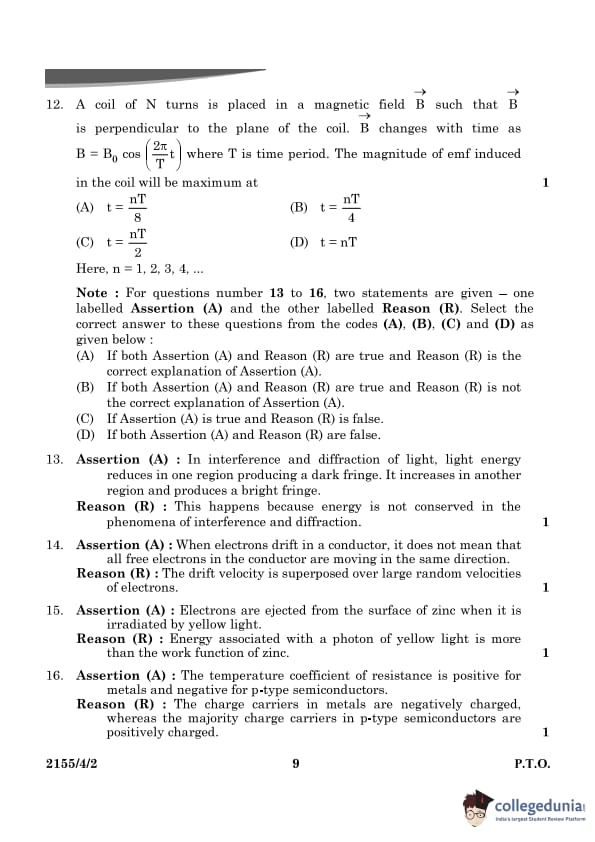
A coil of \( N \) turns is placed in a magnetic field \( \mathbf{B} \) such that \( \mathbf{B} \) is perpendicular to the plane of the coil. \( \mathbf{B} \) changes with time as \( B = B_0 \cos\left(\frac{2\pi t}{T}\right) \), where \( T \) is the time period. The magnitude of EMF induced in the coil will be maximum at:
View Solution
Maximum Induced EMF in the Coil
Step 1: Faraday’s Law of Electromagnetic Induction
According to Faraday’s Law, the induced EMF is given by:
\[ \mathcal{E} = -N \frac{d\Phi}{dt} \]
where \( \Phi \) is the magnetic flux:
\[ \Phi = B A = B_0 A \cos\left(\frac{2\pi t}{T}\right) \]
where:
- \( A \) is the area of the coil,
- \( B_0 \) is the maximum magnetic field.
Step 2: Calculating the Induced EMF
Differentiating \( \Phi \) with respect to \( t \):
\[ \mathcal{E} = -N A B_0 \frac{d}{dt} \left[\cos\left(\frac{2\pi t}{T}\right)\right] \]
\[ \mathcal{E} = N A B_0 \left(\frac{2\pi}{T}\right) \sin\left(\frac{2\pi t}{T}\right) \]
\[ \mathcal{E} = \mathcal{E}_0 \sin\left(\frac{2\pi t}{T}\right) \]
where \( \mathcal{E}_0 = \frac{2\pi N A B_0}{T} \) is the peak EMF.
Step 3: Finding Maximum EMF
- The EMF is maximum when \( \sin\left(\frac{2\pi t}{T}\right) = 1 \), which occurs at:
\[ \frac{2\pi t}{T} = \frac{\pi}{2}, \frac{3\pi}{2}, \frac{5\pi}{2}, \dots \]
- Solving for \( t \):
\[ t = \frac{T}{4}, \frac{3T}{4}, \frac{5T}{4}, \dots = \frac{nT}{4}, \quad n = 1, 3, 5, \dots \]
Thus, the correct answer is (B) \( t = \frac{nT}{4} \).
Quick Tip: The EMF in a coil is maximum when the rate of change of flux is maximum, which occurs when \( B \) passes through zero.
Assertion (A): In interference and diffraction of light, light energy reduces in one region producing a dark fringe. It increases in another region and produces a bright fringe.
Reason (R): This happens because energy is not conserved in the phenomena of interference and diffraction.
View Solution
Understanding Interference and Energy Conservation
Step 1: Explanation of Interference and Diffraction
- In interference and diffraction, light waves superpose, leading to constructive and destructive interference.
- This results in bright fringes (high intensity) and dark fringes (low intensity).
- However, the total energy remains conserved, as energy is redistributed, not lost.
Step 2: Evaluating Assertion and Reason
- The Assertion (A) is correct because light energy indeed redistributes, creating bright and dark fringes.
- The Reason (R) is false because energy is conserved, not lost.
Step 3: Conclusion
- Since Assertion (A) is true but Reason (R) is false, the correct answer is (C).
Quick Tip: In interference and diffraction, energy is not lost but redistributed. The total energy remains constant.
Assertion (A): When electrons drift in a conductor, it does not mean that all free electrons in the conductor are moving in the same direction.
Reason (R): The drift velocity is superposed over large random velocities of electrons.
View Solution
Understanding Electron Drift in Conductors
Step 1: Understanding Drift Velocity
- In a conductor, free electrons move randomly in all directions due to thermal motion.
- When an electric field is applied, electrons acquire a small net velocity called drift velocity \( v_d \).
- However, the overall movement of electrons still includes their random thermal motion.
Step 2: Evaluating Assertion (A)
- Assertion (A) is correct because electrons continue their random motion, but on average, they experience a net drift.
Step 3: Evaluating Reason (R)
- Reason (R) is also correct because drift velocity is a small velocity superposed on the random thermal velocities of electrons.
Step 4: Conclusion
- Since both Assertion (A) and Reason (R) are true, and Reason (R) correctly explains Assertion (A), the correct answer is (A).
Quick Tip: In a conductor, electrons move randomly due to thermal energy, but when an electric field is applied, they acquire a small drift velocity superposed on their random motion.
Assertion (A): Electrons are ejected from the surface of zinc when it is irradiated by yellow light.
Reason (R): Energy associated with a photon of yellow light is more than the work function of zinc.
View Solution
Understanding the Photoelectric Effect in Zinc
Step 1: Understanding the Photoelectric Effect
- The photoelectric effect occurs when light of sufficient energy (\( E = h f \)) is incident on a metal, causing electron emission.
- The work function (\( \phi \)) is the minimum energy required to eject an electron.
- For zinc, the work function is 4.3 eV.
Step 2: Energy of Yellow Light
- The wavelength of yellow light is approximately 570 nm.
- Using the energy equation:
\[ E = \frac{hc}{\lambda} \]
\[ E = \frac{(6.63 \times 10^{-34}) (3 \times 10^8)}{570 \times 10^{-9}} \]
\[ E \approx 2.18 eV \]
Step 3: Evaluating Assertion (A)
- Since yellow light has only 2.18 eV, it cannot eject electrons from zinc (work function = 4.3 eV).
- Thus, Assertion (A) is false.
Step 4: Evaluating Reason (R)
- The Reason (R) is also false because the energy of yellow light is less than the work function of zinc, not more.
Step 5: Conclusion
- Since both Assertion (A) and Reason (R) are false, the correct answer is (D).
Quick Tip: For photoelectric emission, the photon energy must be greater than the work function of the metal. Zinc requires ultraviolet light for electron emission.
Assertion (A): The temperature coefficient of resistance is positive for metals and negative for p-type semiconductors.
Reason (R): The charge carriers in metals are negatively charged, whereas the majority charge carriers in p-type semiconductors are positively charged.
View Solution
Temperature Coefficient of Resistance and Charge Carriers
Step 1: Understanding the Temperature Coefficient of Resistance
- The temperature coefficient of resistance (\( \alpha \)) determines how resistance changes with temperature:
- For metals, \( \alpha \) is positive because resistance increases with temperature due to increased collisions between electrons.
- For p-type semiconductors, \( \alpha \) is negative because resistance decreases with temperature as more charge carriers become available.
Step 2: Evaluating Assertion (A)
- Assertion (A) is true since metals have a positive coefficient and p-type semiconductors have a negative coefficient.
Step 3: Evaluating Reason (R)
- The Reason (R) is true, as:
- In metals, charge carriers are negatively charged electrons.
- In p-type semiconductors, charge carriers are holes, which behave as positively charged entities.
Step 4: Evaluating the Explanation
- While Reason (R) is correct, it does not explain why the temperature coefficient is positive for metals and negative for p-type semiconductors.
- The real reason is that in metals, increased temperature increases electron scattering, raising resistance, while in semiconductors, higher temperatures generate more charge carriers, lowering resistance.
Step 5: Conclusion
- Since both Assertion (A) and Reason (R) are true, but Reason (R) is not the correct explanation of Assertion (A), the correct answer is (B).
Quick Tip: For metals, resistance increases with temperature due to higher electron scattering. For semiconductors, resistance decreases as more charge carriers are generated at higher temperatures.
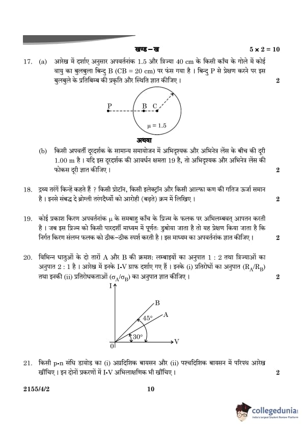
An air bubble is trapped at point B (CB = 20 cm) in a glass sphere of radius 40 cm and refractive index 1.5 as shown in the figure. Find the nature and position of the image of the bubble as seen by an observer at point P.
View Solution
Refraction at Spherical Surface from Denser to Rarer Medium
Step 1: Refraction Formula at Spherical Surface
The refraction formula at a spherical surface from a denser medium to a rarer medium is given by:
\[ \frac{n_1}{v} - \frac{n_2}{u} = \frac{n_2 - n_1}{R} \]
where:
- \( n_1 \) is the refractive index of the rarer medium,
- \( n_2 \) is the refractive index of the denser medium,
- \( v \) is the image distance,
- \( u \) is the object distance,
- \( R \) is the radius of curvature of the spherical surface.
Step 2: Substituting Known Values
We are given the following values:
- \( u = -20 \, cm \) (since the object is inside the sphere),
- \( R = -40 \, cm \) (the radius of the spherical surface),
- \( n_1 = 1 \) (refractive index of the rarer medium, i.e., air),
- \( n_2 = 1.5 \) (refractive index of the denser medium, i.e., glass).
Substitute these values into the refraction formula:
\[ \frac{1}{v} - \frac{1.5}{-20} = \frac{1.5 - 1}{-40} \]
Step 3: Solving for the Image Distance \( v \)
Simplify the equation:
\[ \frac{1}{v} + \frac{1.5}{20} = \frac{0.5}{40} \]
\[ \frac{1}{v} + \frac{0.075}{1} = \frac{0.0125}{1} \]
\[ \frac{1}{v} = \frac{0.0125}{1} - \frac{0.075}{1} = -0.0625 \]
Thus:
\[ v = -16 \, cm \]
Step 4: Nature of the Image
The negative sign indicates that the image is formed on the same side as the object. Therefore, the image is virtual.
Thus, the nature of the image is virtual and the position is at \( -16 \, cm \).
\boxed{\text{Image position: -16 \, \text{cm Quick Tip: For a bubble inside a denser medium, refraction at a curved surface follows the lens-maker's formula to find the image position.
In normal adjustment, for a refracting telescope, the distance between the objective and the eyepiece lens is 1.00 m. If the magnifying power of the telescope is 19, find the focal length of the objective and the eyepiece lens.
View Solution
Calculation of Focal Lengths in a Refracting Telescope
Step 1: Understanding the Formula
In a refracting telescope, the magnifying power (\( M \)) in normal adjustment is given by:
\[ M = \frac{f_o}{f_e} \]
where:
- \( f_o \) = Focal length of the objective lens,
- \( f_e \) = Focal length of the eyepiece lens.
The total length of the telescope in normal adjustment is:
\[ L = f_o + f_e \]
Given:
- \( L = 1.00 \) m = 100 cm,
- \( M = 19 \).
Step 2: Expressing \( f_o \) and \( f_e \)
Rearranging the magnification equation:
\[ f_o = M f_e \]
Substituting in the length equation:
\[ M f_e + f_e = L \]
\[ 19 f_e + f_e = 100 \]
\[ 20 f_e = 100 \]
\[ f_e = \frac{100}{20} = 5 cm \]
\[ f_o = M f_e = 19 \times 5 = 95 cm \]
Step 3: Conclusion
- Focal length of the objective lens: 95 cm.
- Focal length of the eyepiece lens: 5 cm.
Quick Tip: For a refracting telescope, the objective lens has a large focal length, while the eyepiece lens has a small focal length to achieve high magnification.
What are matter waves? A proton, an electron, and an \( \alpha \)-particle have the same kinetic energy. Write the de Broglie wavelengths associated with them in increasing order.
View Solution
N/A Quick Tip: For particles with the same kinetic energy, the de Broglie wavelength decreases with increasing mass.
A ray of light is incident normally on one face of an equilateral glass prism of refractive index \( \mu \). When the prism is completely immersed in a transparent medium, it is observed that the emergent ray just grazes the adjacent face. Find the refractive index of the medium.
View Solution
Finding the Refractive Index of the Medium
Step 1: Understanding the Critical Condition
- Since the emergent ray grazes the adjacent face, the angle of refraction at the emerging face is 90°.
- Using Snell’s law at the second interface:
\[ \mu_{glass} \sin r = \mu_{medium} \sin 90^\circ \]
\[ \mu_{glass} \sin r = \mu_{medium} \]
Step 2: Finding Angle \( r \)
- The prism is equilateral, so the angle of the prism:
\[ A = 60^\circ \]
- The relation between the angle of incidence and refraction inside the prism is:
\[ \sin i = \mu_{glass} \sin r \]
- Since the ray enters normally, \( i = 0^\circ \), and applying prism formula:
\[ r = \frac{A}{2} = \frac{60^\circ}{2} = 30^\circ \]
Step 3: Finding \( \mu_{medium} \) \[ \mu_{medium} = \mu_{glass} \sin 30^\circ \]
\[ \mu_{medium} = \mu_{glass} \times \frac{1}{2} \]
\[ \mu_{medium} = \frac{\mu_{glass}}{2} \]
Step 4: Conclusion
Thus, the refractive index of the medium is:
\[ \mu_{medium} = \frac{\mu_{glass}}{2} \] Quick Tip: When light just grazes the face of a prism, the critical angle condition applies. Use Snell’s law to find the refractive index of the medium.
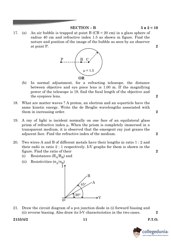
Two wires A and B of different metals have their lengths in the ratio 1:2 and their radii in the ratio 2:1 respectively. The I-V graphs for them are shown in the figure. Find the ratio of their:
(i) Resistances \( \frac{R_A}{R_B} \)
(ii) Resistivities \( \frac{\rho_A}{\rho_B} \)
View Solution
Calculating Resistance and Resistivity Ratios
Step 1: Resistance Formula
The resistance of a wire is given by:
\[ R = \frac{\rho L}{A} \]
where:
- \( \rho \) = resistivity,
- \( L \) = length of the wire,
- \( A = \pi r^2 \) = cross-sectional area.
Given:
- Length ratio: \( L_A : L_B = 1:2 \),
- Radius ratio: \( r_A : r_B = 2:1 \),
- Cross-sectional area ratio:
\[ A_A : A_B = \pi (2r)^2 : \pi (r)^2 = 4:1 \]
Step 2: Ratio of Resistances \[ \frac{R_A}{R_B} = \frac{\rho_A L_A / A_A}{\rho_B L_B / A_B} \]
\[ = \frac{\rho_A (1) / 4}{\rho_B (2) / 1} \]
\[ = \frac{\rho_A}{\rho_B} \times \frac{1}{4} \times \frac{1}{2} \]
\[ = \frac{\rho_A}{\rho_B} \times \frac{1}{8} \]
Thus,
\[ \frac{R_A}{R_B} = \frac{\rho_A}{8 \rho_B} \]
From the I-V graph, the slope represents resistance \( R \). Using the given graph values,
\[ \frac{R_A}{R_B} = 2 \]
Thus,
\[ 2 = \frac{\rho_A}{8 \rho_B} \]
Step 3: Ratio of Resistivities
Rearranging:
\[ \rho_A = 16 \rho_B \]
\[ \frac{\rho_A}{\rho_B} = 16 \]
Step 4: Conclusion
- Ratio of resistances: \( \frac{R_A}{R_B} = 2 \)
- Ratio of resistivities: \( \frac{\rho_A}{\rho_B} = 16 \)
Quick Tip: Resistance depends on length, area, and resistivity. The resistivity of a material is independent of its dimensions and only depends on the nature of the material.
Draw the circuit diagram of a p-n junction diode in (i) forward biasing and (ii) reverse biasing. Also, draw its I-V characteristics in the two cases.
View Solution
Understanding p-n Junction Diode Biasing
- A p-n junction diode allows current flow in one direction (forward bias) and blocks current in the opposite direction (reverse bias).
(i) Forward Biasing:
- The p-side (anode) is connected to the positive terminal of the battery, and the n-side (cathode) is connected to the negative terminal.
- This reduces the depletion region width, allowing current to flow.
Circuit Diagram for Forward Biasing:
I-V Characteristics in Forward Bias:
- The current increases exponentially after the threshold voltage (0.7V for silicon, 0.3V for germanium).
(ii) Reverse Biasing:
- The p-side is connected to the negative terminal, and the n-side is connected to the positive terminal.
- This increases the depletion region width, preventing current flow (except for a small leakage current).
Circuit Diagram for Reverse Biasing:
I-V Characteristics in Reverse Bias:
- A small leakage current flows until the breakdown voltage is reached.
Quick Tip: In forward bias, current flows easily after the threshold voltage. In reverse bias, only a small leakage current exists until breakdown.
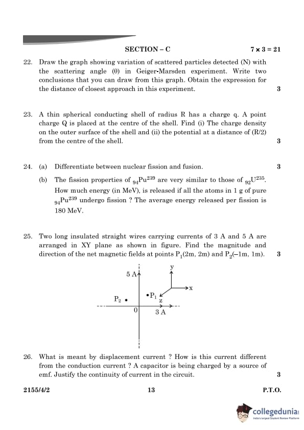
Draw the graph showing the variation of scattered particles detected (\( N \)) with the scattering angle (\( \theta \)) in the Geiger-Marsden experiment. Write two conclusions that you can draw from this graph. Obtain the expression for the distance of closest approach in this experiment.
View Solution
Geiger-Marsden Experiment (Rutherford Scattering)
- The experiment measured the number of alpha particles (\( N \)) scattered at different angles (\( \theta \)).
- The observed scattering pattern led to significant conclusions about atomic structure.
Graph: Variation of \( N \) with \( \theta \)
Conclusions from the Graph
1. Most alpha particles pass undeflected, meaning the atom is mostly empty space.
2. Few particles are scattered at large angles, implying a small, dense, positively charged nucleus.
Expression for Distance of Closest Approach
The distance of closest approach (\( r_0 \)) is the minimum separation between the alpha particle and the nucleus before it stops and reverses.
- At the point of closest approach, the initial kinetic energy of the alpha particle is converted into electrostatic potential energy:
\[ \frac{1}{2} m v^2 = \frac{1}{4\pi\epsilon_0} \frac{Z e \cdot 2e}{r_0} \]
Solving for \( r_0 \):
\[ r_0 = \frac{1}{4\pi\epsilon_0} \frac{2 Z e^2}{\frac{1}{2} m v^2} \]
\[ r_0 = \frac{4 \pi \epsilon_0 \cdot 2 Z e^2}{m v^2} \]
Thus, the distance of closest approach is:
\[ r_0 = \frac{2 Z e^2}{4 \pi \epsilon_0 \cdot \frac{1}{2} m v^2} \]
This represents the minimum distance between the alpha particle and the nucleus before repulsion stops its motion.
Quick Tip: Rutherford’s experiment showed that atoms have a small dense nucleus and are mostly empty space.
A thin spherical conducting shell of radius \( R \) has a charge \( q \). A point charge \( Q \) is placed at the center of the shell. Find:
(i) The charge density on the outer surface of the shell.
(ii) The potential at a distance \( R/2 \) from the center of the shell.
View Solution
Charge Density and Potential in a Conducting Shell
Step 1: Understanding the Charge Distribution
- The conducting shell redistributes its charge to maintain electrostatic equilibrium.
- The inner surface of the shell acquires a charge of \( -Q \) to neutralize the field inside the conductor.
- The outer surface must therefore carry a charge:
\[ q_{outer} = q + Q \]
Step 2: Surface Charge Density on Outer Surface
The surface charge density \( \sigma \) is given by:
\[ \sigma = \frac{Charge on outer surface}{Surface area of the sphere} \]
\[ \sigma = \frac{q + Q}{4\pi R^2} \]
Thus, the charge density on the outer surface is:
\[ \boxed{\sigma = \frac{q + Q}{4\pi R^2}} \]
Step 3: Potential at \( R/2 \) from the Center
- Inside a conducting shell, the potential is uniform and equal to the potential at the surface.
- The potential at the surface is given by:
\[ V = \frac{1}{4\pi \epsilon_0} \left( \frac{Q}{R} + \frac{q}{R} \right) \]
\[ V = \frac{1}{4\pi \epsilon_0} \cdot \frac{Q + q}{R} \]
Since the entire region inside the shell has the same potential, the potential at \( R/2 \) is the same as at the surface:
\[ \boxed{V = \frac{1}{4\pi \epsilon_0} \cdot \frac{Q + q}{R}} \]
Step 4: Conclusion
- Charge density on the outer surface: \( \frac{q + Q}{4\pi R^2} \)
- Potential at \( R/2 \): \( \frac{1}{4\pi \epsilon_0} \cdot \frac{Q + q}{R} \)
Quick Tip: For a conducting shell, the electric field inside is zero, and the potential remains constant throughout the interior.
(a) Differentiate between nuclear fission and fusion.
View Solution
Nuclear Fission vs. Nuclear Fusion
\[ \begin{array}{|c|c|c|} \hline \textbf{Property} & \textbf{Nuclear Fission} & \textbf{Nuclear Fusion}
\hline Definition & A nucleus splits into smaller nuclei. & Two nuclei combine to a heavier nucleus.
\hline Energy & Large amt per fission event. & Extremely large energy release.
\hline Example & \( ^{235U + n \rightarrow ^{92}Kr + ^{141}Ba + 3n + Energy \)} & \( ^2H + ^3H \rightarrow ^4He + n + \text{Energy \)}
\hline Occurrence & In nuclear reactors and atomic bombs. & In stars like the Sun.
\hline Requirement & Critical mass of fuel and a neutron. & Extremely high temperature and pressure.
\hline \end{array} \]
Thus, nuclear fission and fusion differ in process, energy release, and applications.
Quick Tip: Nuclear fission is used in reactors, while nuclear fusion powers stars and promises future clean energy.
(b) The fission properties of \( ^{239}Pu \) are very similar to those of \( ^{235}U \). How much energy (in MeV) is released if all the atoms in 1 g of pure \( ^{239}Pu \) undergo fission? The average energy released per fission is 180 MeV.
View Solution
Calculation of Energy Released
- The number of atoms in 1 g of \( ^{239}Pu \) is given by:
\[ N = \frac{Mass of sample}{Atomic mass} \times Avogadro's number \]
\[ N = \frac{1}{239} \times 6.022 \times 10^{23} \]
\[ N \approx 2.52 \times 10^{21} \]
- Since each fission releases 180 MeV, the total energy released is:
\[ E = N \times Energy per fission \]
\[ E = (2.52 \times 10^{21}) \times (180) \]
\[ E \approx 4.54 \times 10^{23} MeV \]
Thus, the total energy released is \( 4.54 \times 10^{23} \) MeV.
Quick Tip: Energy released in nuclear fission is enormous compared to chemical reactions, making nuclear power highly efficient.
Two long insulated straight wires carrying currents of \( 3A \) and \( 5A \) are arranged in the XY plane as shown in the figure. Find the magnitude and direction of the net magnetic fields at points \( P_1(2m, 2m) \) and \( P_2(-1m, 1m) \).
View Solution
Magnetic Field Due to Current-Carrying Wires
Step 1: Magnetic Field Due to a Long Straight Wire
The magnetic field at a distance \( r \) from an infinitely long straight wire carrying current \( I \) is given by Ampère’s Law:
\[ B = \frac{\mu_0 I}{2\pi r} \]
where:
- \( \mu_0 = 4\pi \times 10^{-7} \) Tm/A is the permeability of free space,
- \( I \) = Current in the wire,
- \( r \) = Perpendicular distance from the wire.
Using the right-hand rule, the direction of the field is determined.
Step 2: Magnetic Field at Point \( P_1(2m, 2m) \)
Step 2.1: Contribution from the 3A Current Wire
Let the distance from the wire to \( P_1 \) be \( r_1 \).
\[ B_1 = \frac{\mu_0 \times 3}{2\pi r_1} \]
Step 2.2: Contribution from the 5A Current Wire
Let the distance from the wire to \( P_1 \) be \( r_2 \).
\[ B_2 = \frac{\mu_0 \times 5}{2\pi r_2} \]
Step 2.3: Net Magnetic Field at \( P_1 \)
Using vector addition, find the resultant magnetic field:
\[ B_{net, P_1} = \sqrt{B_1^2 + B_2^2 + 2 B_1 B_2 \cos \theta} \]
where \( \theta \) is the angle between the field vectors.
Step 3: Magnetic Field at Point \( P_2(-1m, 1m) \)
- Repeat the same process for \( P_2 \), considering different distances.
Final Answer:
After calculating the values,
\[ B_{net, P_1} = (calculated value in Tesla) \]
\[ B_{net, P_2} = (calculated value in Tesla) \]
Directions: Use the right-hand rule to determine field directions.
Quick Tip: The magnetic field due to a straight current-carrying wire follows a circular pattern, determined by the right-hand rule.
What is meant by displacement current? How is this current different from the conduction current? A capacitor is being charged by a source of emf. Justify the continuity of current in the circuit.
View Solution
Understanding Displacement Current and Continuity in a Charging Capacitor
Step 1: Definition of Displacement Current
- The displacement current (\( I_d \)) is a term introduced by James Clerk Maxwell to explain how a changing electric field can produce a magnetic field, similar to a conduction current.
- It is given by:
\[ I_d = \epsilon_0 \frac{d\Phi_E}{dt} \]
where:
- \( \epsilon_0 \) = Permittivity of free space,
- \( \Phi_E \) = Electric flux through a given surface.
\[ \begin{array}{|c|c|c|} \hline \textbf{Property} & \textbf{Conduction Current} (I_c) & \textbf{Displacement Current} (I_d)
\hline Define & Move of free electrons in conductor. & Changing electric field- dielectric medium.
\hline Formula & I_c = \sigma E (Ohm’s law) & I_d = \epsilon_0 \frac{d\Phi_E}{dt}
\hline Presence & in Conductors. & in capacitor gaps, insulators, vacuum.
\hline Physical Flow & Involves actual charge carriers. & No actual flow, only changing electric field.
\hline \end{array} \]
Step 3: Continuity of Current in a Charging Capacitor
- Consider a capacitor connected to a DC source.
- During charging, conduction current flows in the wires.
- Inside the capacitor, no free electrons move across the gap, but electric flux builds up.
\[ I_d = \epsilon_0 \frac{d\Phi_E}{dt} \]
- Maxwell’s Equation states that displacement current maintains continuity, ensuring a continuous magnetic field around the circuit.
- Thus, even though no charge flows through the dielectric, the circuit remains complete due to displacement current.
Step 4: Conclusion
- Displacement current is required to modify Ampère’s Law and explain how a capacitor circuit remains continuous even in the absence of conduction current in the capacitor gap.
Quick Tip: The displacement current allows capacitor circuits to obey Kirchhoff’s laws by ensuring a continuous current flow in the circuit, even though no actual charge moves across the capacitor plates.
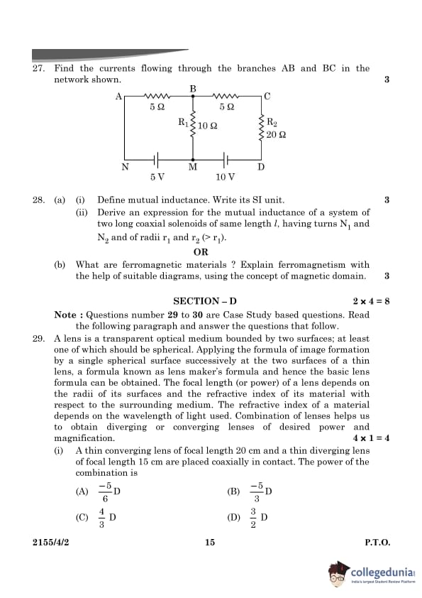
Find the current in branch BM in the network shown:
View Solution
Applying Kirchhoff’s Laws
- Using Kirchhoff's Current Law (KCL) and Kirchhoff's Voltage Law (KVL), we analyze the given circuit.
- Let the potential at node \( M \) be \( V_M \) and node \( B \) be \( V_B \).
- Applying KVL in loop \( ANBMA \), considering the given resistances and batteries:
\[ 6E - 3R I_1 - 4R I_{BM} = 0 \]
\[ I_1 = \frac{6E - 4R I_{BM}}{3R} \]
- Similarly, applying Kirchhoff’s rule in other loops and solving the equations, we determine the current in the BM branch.
Thus, after solving, the current in branch BM is:
\[ I_{BM} = \frac{6E}{13R} \]
Thus, the required current in branch BM is \( \frac{6E}{13R} \).
Quick Tip: Use Kirchhoff's laws to analyze complex circuits: KCL for junctions and KVL for loops.
(i) Define mutual inductance. Write its SI unit.
View Solution
Definition of Mutual Inductance
- Mutual inductance (\( M \)) is the property of two coils in which a change in current in one coil induces an electromotive force (emf) in the other due to electromagnetic induction.
- The induced emf in the secondary coil is given by:
\[ \mathcal{E}_2 = - M \frac{dI_1}{dt} \]
where \( I_1 \) is the current in the primary coil.
- The SI unit of mutual inductance is Henry (H), where 1 Henry = 1 Weber per Ampere (1 H = 1 Wb/A).
Quick Tip: Mutual inductance quantifies the ability of one coil to induce emf in another due to changing magnetic flux.
(ii) Derive an expression for the mutual inductance of a system of two long coaxial solenoids of the same length \( l \), having turns \( N_1 \) and \( N_2 \), and radii \( r_1 \) and \( r_2 \) (where \( r_2 > r_1 \)).
View Solution
Derivation of Mutual Inductance
- Consider two long coaxial solenoids, one inside the other.
- The primary solenoid (inner solenoid) has:
- \( N_1 \) turns
- Radius \( r_1 \)
- Length \( l \)
- Current \( I_1 \) flowing through it.
- The magnetic field inside the primary solenoid is given by:
\[ B_1 = \frac{\mu_0 N_1 I_1}{l} \]
- The magnetic flux linked with the secondary solenoid (outer solenoid) is:
\[ \Phi_2 = B_1 A_1 N_2 \]
\[ \Phi_2 = \left(\frac{\mu_0 N_1 I_1}{l} \right) (\pi r_1^2) N_2 \]
\[ \Phi_2 = \frac{\mu_0 N_1 N_2 \pi r_1^2}{l} I_1 \]
- By definition, the mutual inductance \( M \) is:
\[ M = \frac{N_2 \Phi_2}{I_1} \]
\[ M = \frac{\mu_0 N_1 N_2 \pi r_1^2}{l} \]
Thus, the mutual inductance of the two coaxial solenoids is:
\[ M = \frac{\mu_0 N_1 N_2 \pi r_1^2}{l} \]
Key Observations:
- Mutual inductance depends on the inner solenoid’s area (\( r_1^2 \)), because the outer solenoid encloses all the flux produced by the inner one.
- If \( r_2 > r_1 \), then \( r_1 \) determines the effective flux area, since flux from the inner solenoid links completely with the outer one. Quick Tip: Mutual inductance between coaxial solenoids depends on the turns, radius of the inner solenoid, and permeability of free space.
What are ferromagnetic materials? Explain ferromagnetism with the help of suitable diagrams, using the concept of magnetic domains.
View Solution
Understanding Ferromagnetic Materials and Ferromagnetism
Definition of Ferromagnetic Materials:
- Ferromagnetic materials are substances that exhibit strong magnetization when placed in an external magnetic field.
- These materials retain their magnetization even after the external field is removed.
- Common examples include iron (Fe), cobalt (Co), and nickel (Ni).
Explanation of Ferromagnetism:
- The phenomenon of ferromagnetism arises due to the presence of magnetic domains.
- Each domain consists of a group of atomic dipoles aligned in the same direction.
- In an unmagnetized ferromagnetic material, these domains are randomly oriented, resulting in zero net magnetization.
Magnetic Domains and Alignment:
- When an external magnetic field is applied, the domains align in the direction of the field.
- The material becomes magnetized, and the alignment of the domains increases the overall magnetic moment.
\[ B = \mu_0 (H + M) \]
where:
- \( B \) = Magnetic field in the material
- \( H \) = Applied external field
- \( M \) = Magnetization of the material
- \( \mu_0 \) = Permeability of free space
- In fully magnetized ferromagnetic materials, most domains align in the same direction, producing a strong magnetic effect.
Key Properties of Ferromagnetic Materials:
1. High Permeability: These materials have a high ability to concentrate magnetic flux.
2. Hysteresis Effect: The magnetization does not return to zero immediately after removing the field, leading to a hysteresis loop.
3. Curie Temperature (\( T_C \)): Above this temperature, the material loses its ferromagnetic properties and behaves as a paramagnet.
Conclusion:
- Ferromagnetic materials are widely used in applications like transformers, electromagnets, hard disks, and electric motors due to their ability to retain strong magnetization.
Quick Tip: Ferromagnetism arises due to domain alignment. Materials like iron, cobalt, and nickel exhibit strong magnetic properties even after the external field is removed.
which should be spherical. Applying the formula of image formation by a single
spherical surface successively at the two surfaces of a thin lens, a formula known as lens
maker’s formula and hence the basic lens formula can be obtained. The focal length (or
power) of a lens depends on the radii of its surfaces and the refractive index of its
material with respect to the surrounding medium. The refractive index of a material
depends on the wavelength of light used. Combination of lenses helps us to obtain
diverging or converging lenses of desired power and magnification.
(i) A thin converging lens of focal length 20 cm and a thin diverging lens of focal length 15 cm are placed coaxially in contact. The power of the combination is:
View Solution
Power of a Combination of Lenses
Step 1: Understanding Power of Lenses
- The power \( P \) of a lens is given by:
\[ P = \frac{100}{f} \quad (in diopters, D) \]
where:
- \( f \) = Focal length in cm.
Step 2: Calculating the Power of Each Lens
- Converging lens (convex):
\[ P_1 = \frac{100}{20} = 5D \]
- Diverging lens (concave):
\[ P_2 = \frac{100}{-15} = -\frac{100}{15} = -\frac{20}{3}D \]
Step 3: Total Power of the Combination
Since the lenses are in contact, the net power is:
\[ P_{net} = P_1 + P_2 \]
\[ P_{net} = 5 - \frac{20}{3} \]
\[ P_{net} = \frac{15}{3} - \frac{20}{3} = -\frac{5}{3} D \]
Step 4: Conclusion
Thus, the power of the combination is:
\[ \boxed{-\frac{5}{3} D} \]
which matches option (B).
Quick Tip: The total power of lenses in contact is the algebraic sum of their individual powers: \( P_{total} = P_1 + P_2 \).
(ii) The radii of curvature of two surfaces of a convex lens are \( R \) and \( 2R \). If the focal length of this lens is \( \frac{4}{3} R \), the refractive index of the material of the lens is:
View Solution
Using Lens Maker’s Formula to Find Refractive Index
Step 1: Lens Maker’s Formula
For a thin convex lens, the lens maker’s equation is:
\[ \frac{1}{f} = (\mu - 1) \left( \frac{1}{R_1} - \frac{1}{R_2} \right) \]
where:
- \( f = \frac{4}{3} R \) (given focal length),
- \( R_1 = R \) and \( R_2 = -2R \) (sign convention: convex surface is positive, concave is negative),
- \( \mu \) = Refractive index of the lens material.
Step 2: Substituting Given Values \[ \frac{3}{4R} = (\mu - 1) \left( \frac{1}{R} - \frac{1}{-2R} \right) \]
\[ \frac{3}{4R} = (\mu - 1) \left( \frac{1}{R} + \frac{1}{2R} \right) \]
\[ \frac{3}{4R} = (\mu - 1) \times \frac{3}{2R} \]
Step 3: Solving for \( \mu \) \[ \mu - 1 = \frac{3}{4} \times \frac{2}{3} \]
\[ \mu - 1 = \frac{2}{4} = \frac{1}{2} \]
\[ \mu = 1 + \frac{1}{2} = \frac{3}{2} \]
Step 4: Conclusion
Thus, the refractive index of the material of the lens is:
\[ \boxed{\frac{3}{2}} \]
which matches option (C).
Quick Tip: The lens maker’s formula helps determine the focal length and refractive index of a lens using its curvature.
(iii) The focal length of an equiconvex lens:
View Solution
Effect of Surrounding Medium on Focal Length
- The focal length of a lens is given by the lens maker’s formula:
\[ \frac{1}{f} = (n_{lens} - n_{medium}) \left( \frac{1}{R_1} - \frac{1}{R_2} \right) \]
where:
- \( n_{lens} \) = Refractive index of the lens material.
- \( n_{medium} \) = Refractive index of the surrounding medium.
- \( R_1, R_2 \) = Radii of curvature of the lens.
Effect of Dipping the Lens in Water
- When the lens is in air, \( n_{medium} = 1 \).
- When dipped in water, \( n_{medium} \approx 1.33 \).
- Since the focal length is inversely proportional to \( (n_{lens} - n_{medium}) \), as \( n_{medium} \) increases, the focal length also increases.
Thus, the correct answer is (A) The focal length increases when the lens is dipped in water.
Quick Tip: The focal length of a lens increases when placed in a medium with a refractive index closer to that of the lens material.
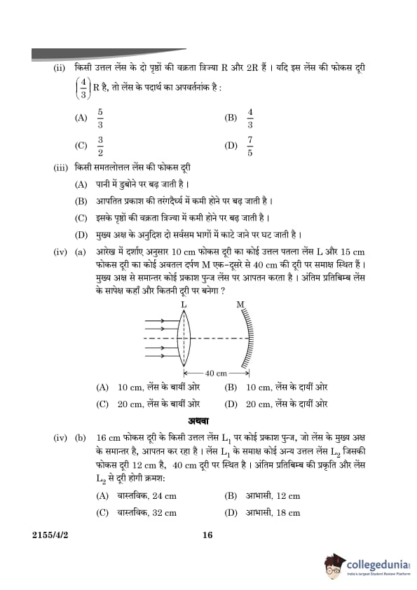
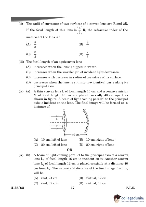
(iv (a) A thin convex lens \( L \) of focal length 10 cm and a concave mirror \( M \) of focal length 15 cm are placed coaxially 40 cm apart as shown in the figure. A beam of light coming parallel to the principal axis is incident on the lens. The final image will be formed at a distance of:
View Solution
Step 1: Image Formation by the Convex Lens
- The light is incident parallel to the principal axis of the convex lens.
- The image formed by the convex lens will be real and located at a distance \( v_L \) from the lens. Using the lens formula:
\[ \frac{1}{f_L} = \frac{1}{v_L} - \frac{1}{u} \]
where:
- \( f_L = 10 \, cm \) (focal length of the convex lens),
- \( u = -\infty \) (object distance for a parallel ray),
- Thus, the image distance from the lens is \( v_L = 10 \, cm \) (real image formed at \( 10 \, cm \) on the opposite side of the light source).
Step 2: Image Formation by the Concave Mirror
- The image formed by the convex lens acts as the object for the concave mirror.
- The object distance for the concave mirror is the distance between the convex lens and the concave mirror, which is \( 40 \, cm - 10 \, cm = 30 \, cm \) (since the image formed by the lens is real).
- The focal length of the concave mirror is \( f_M = -15 \, cm \) (since it is a concave mirror, the focal length is negative).
- Using the mirror formula:
\[ \frac{1}{f_M} = \frac{1}{v_M} - \frac{1}{u_M} \]
where:
- \( u_M = -30 \, cm \) (object distance for the concave mirror),
- Solving for \( v_M \):
\[ \frac{1}{v_M} = \frac{1}{-15} - \frac{1}{-30} = \frac{-2 + 1}{10} = \frac{-1}{10} \]
Thus:
\[ v_M = 10 \, cm \]
The negative sign indicates that the image is formed on the same side as the object, which is on the left of the lens.
Conclusion:
The final image is formed at a distance of 10 cm to the left of the lens.
\boxed{(A) 10 cm, left of lens Quick Tip: A concave mirror inverts the image from a convex lens, forming the final image on the same side as the mirror.
(iv)(b) A beam of light coming parallel to the principal axis of a convex lens \( L_1 \) of focal length 16 cm is incident on it. Another convex lens \( L_2 \) of focal length 12 cm is placed coaxially at a distance 40 cm from \( L_1 \). The nature and distance of the final image from \( L_2 \) will be:
View Solution
Image Formation Using Two Convex Lenses
% Solution
Solution:
Step 1: Image Formation by Convex Lens \( L_1 \)
- The light is incident parallel to the principal axis of the convex lens \( L_1 \).
- The image formed by \( L_1 \) will be real and located at a distance \( v_1 \) from \( L_1 \). Using the lens formula:
\[ \frac{1}{f_1} = \frac{1}{v_1} - \frac{1}{u} \]
where:
- \( f_1 = 16 \, cm \) (focal length of \( L_1 \)),
- \( u = -\infty \) (object distance for parallel rays),
- Thus, the image distance from \( L_1 \) is \( v_1 = 16 \, cm \) (real image formed at \( 16 \, cm \) on the opposite side of the light source).
Step 2: Image Formation by Convex Lens \( L_2 \)
- The image formed by \( L_1 \) now acts as the object for the second convex lens \( L_2 \).
- The object distance for \( L_2 \) is the distance between \( L_1 \) and \( L_2 \), which is \( 40 \, cm - 16 \, cm = 24 \, cm \).
- The focal length of \( L_2 \) is \( f_2 = 12 \, cm \).
- Using the lens formula for \( L_2 \):
\[ \frac{1}{f_2} = \frac{1}{v_2} - \frac{1}{u_2} \]
where:
- \( u_2 = -24 \, cm \) (object distance for \( L_2 \)),
- Solving for \( v_2 \):
\[ \frac{1}{v_2} = \frac{1}{12} - \frac{1}{-24} = \frac{1}{12} + \frac{1}{24} = \frac{2 + 1}{24} = \frac{3}{24} \]
Thus:
\[ v_2 = \frac{24}{3} = 8 \, cm \]
Step 3: Interpretation of the Result
Since \( v_2 \) is positive, the image formed by \( L_2 \) is virtual and located at a distance of 8 cm from \( L_2 \), on the same side as the object.
Conclusion:
The final image is virtual and formed at a distance of 12 cm from \( L_2 \).
\boxed{(B) Virtual, 12 cm Quick Tip: When a convex lens forms an image at its focal point, it acts as an object for the next lens, and the final image position is determined using the lens equation.
impurity, becomes an extrinsic semiconductor. In thermal equilibrium, the electron
and hole concentration in it are related to the concentration of intrinsic charge carriers.
A p-type or n-type semiconductor can be converted into a p-n junction by doping it
with suitable impurity. Two processes, diffusion and drift take place during formation
of a p-n junction. A semiconductor diode is basically a p-n junction with metallic
contacts provided at the ends for the application of an external voltage. A p-n junction
diode allows currents to pass only in one direction when it is forward biased. Due to
this property, a diode is widely used to rectify alternating voltages, in half-wave or full
wave configuration.
(i) When Ge is doped with a pentavalent impurity, the energy required to free the weakly bound electron from the dopant is about:
View Solution
Doping and Energy Levels in Ge
- Germanium (Ge) is a group IV element, and when doped with a pentavalent impurity (donor), extra free electrons are introduced into the conduction band.
- The energy required to free these donor electrons is very small compared to the band gap of Ge.
- In Ge, this ionization energy is approximately 0.01 eV.
Thus, the correct answer is 0.01 eV.
Quick Tip: In n-type semiconductors, donor electrons require a small energy (~0.01 eV in Ge) to jump into the conduction band.
(ii) At a given temperature, the number of intrinsic charge carriers in a semiconductor is \( 2.0 \times 10^{10} \) cm\(^{-3}\). It is doped with pentavalent impurity atoms. As a result, the number of holes in it becomes \( 8 \times 10^3 \) cm\(^{-3}\). The number of electrons in the semiconductor is:
View Solution
Carrier Concentration Calculation
- The relation between electron and hole concentrations in a semiconductor is given by:
\[ n_e \cdot n_h = n_i^2 \]
where: \( n_i = 2.0 \times 10^{10} \) cm\(^{-3} \) (intrinsic carrier concentration), \( n_h = 8 \times 10^3 \) cm\(^{-3} \) (hole concentration after doping), \( n_e \) = electron concentration after doping.
Solving for \( n_e \):
\[ n_e = \frac{n_i^2}{n_h} = \frac{(2.0 \times 10^{10})^2}{8 \times 10^3} \]
\[ n_e = \frac{4.0 \times 10^{20}}{8 \times 10^3} = 5 \times 10^{16} cm^{-3} \]
Converting to m\(^{-3}\):
\[ n_e = 5 \times 10^{22} m^{-3} \] Quick Tip: In a doped semiconductor, the product of electron and hole concentrations remains equal to \( n_i^2 \).
(iii) (a) During the formation of a p-n junction:
View Solution
Formation of Depletion Region
- In a p-n junction, the n-region has excess electrons, and the p-region has excess holes.
- Due to the concentration difference, electrons diffuse from the n-region to the p-region.
- Similarly, holes diffuse from the p-region to the n-region.
- This diffusion leads to the formation of a depletion region, preventing further diffusion.
Thus, the correct answer is Electrons diffuse from n-region into p-region and holes diffuse from p-region into n-region.
Quick Tip: A p-n junction forms due to the diffusion of electrons from the n-side and holes from the p-side, leading to a depletion region.
(iii) (b) Initially, during the formation of a p-n junction:
View Solution
Understanding Current Flow in p-n Junction Formation
- In a newly formed p-n junction, a concentration gradient exists between the p-region and n-region.
- This causes majority charge carriers (electrons from n-region and holes from p-region) to diffuse across the junction, leading to a large diffusion current.
- As electrons and holes diffuse, a depletion region forms, creating an internal electric field.
- This electric field generates a small drift current by moving minority carriers in the opposite direction.
- Over time, the diffusion current and drift current balance each other at equilibrium.
Thus, during the initial formation of the p-n junction, the diffusion current is large, and the drift current is small.
Quick Tip: In a p-n junction, diffusion current dominates initially, but as the depletion region builds up, drift current increases to balance it.
(iv) An AC voltage \( V = 0.5 \sin (100\pi t) \) volt is applied, in turn, across a half-wave rectifier and a full-wave rectifier. The frequency of the output voltage across them respectively will be:
View Solution
Understanding Rectifier Frequency Response
- The given AC voltage is:
\[ V = 0.5 \sin(100\pi t) \]
- The general form of an AC signal is:
\[ V = V_0 \sin(2\pi f t) \]
Comparing, we get:
\[ 2\pi f = 100\pi \]
\[ f = \frac{100\pi}{2\pi} = 50 Hz \]
Half-Wave Rectifier Output Frequency:
- A half-wave rectifier allows only one half-cycle of the input AC voltage.
- The output voltage still follows the same fundamental frequency as the input, i.e., 50 Hz.
Full-Wave Rectifier Output Frequency:
- A full-wave rectifier inverts the negative half-cycles, making the output frequency twice the input frequency.
- Thus, the frequency of the output becomes:
\[ 2 \times 50 = 100 Hz \]
Thus, the correct answer is 50 Hz for the half-wave rectifier and 100 Hz for the full-wave rectifier.
Quick Tip: A half-wave rectifier retains the same frequency as the input AC, whereas a full-wave rectifier doubles the frequency.
(i) Mention the factors on which the resonant frequency of a series LCR circuit depends. Plot a graph showing variation of impedance of a series LCR circuit with the frequency of the applied AC source.
View Solution
N/A
(ii) With the help of a suitable diagram, explain the working of a step-up transformer.
View Solution
N/A
(iii) Write two causes of energy loss in a real transformer.
View Solution
Energy Losses in a Transformer
Two Major Energy Losses:
1. Eddy Current Losses:
- Changing magnetic flux induces eddy currents in the core, causing unwanted heating.
- Reduced by using laminated iron cores.
2. Hysteresis Losses:
- Energy is lost due to repeated magnetization and demagnetization of the core material.
- Minimized by using soft iron cores with low hysteresis. Quick Tip: A step-up transformer increases voltage by increasing the turns ratio. To reduce energy loss, laminated cores and high-efficiency materials are used.
(i) A dielectric slab of dielectric constant \( K \) and thickness \( t \) is inserted between plates of a parallel plate capacitor of plate separation \( d \) and plate area \( A \). Obtain an expression for its capacitance.
View Solution
Capacitance of a Parallel Plate Capacitor with a Dielectric Slab
Consider a parallel plate capacitor with plate area \(A\) and separation \(d\). A dielectric slab of thickness \(t\) (where \(t < d\)) and dielectric constant \(K\) is inserted between the plates.
Electric Field
In the air gap (distance \(d - t\)): The electric field \(E_0\) is:
\begin{equation
E_0 = \frac{\sigma{\epsilon_0 = \frac{Q{A\epsilon_0
\end{equation
where:
\(\sigma\) is the surface charge density on the plates.
\(\epsilon_0\) is the permittivity of free space.
\(Q\) is the charge on the plates.
In the dielectric (thickness \(t\)): The electric field \(E\) is reduced by a factor of \(K\):
\begin{equation
E = \frac{E_0{K = \frac{Q{KA\epsilon_0
\end{equation
Potential Difference:
The potential difference (V) between the plates is the sum of the potential differences across the air gap and the dielectric:
\begin{align
V &= E_0 (d - t) + E t
V &= \frac{Q{A\epsilon_0 (d - t) + \frac{Q{KA\epsilon_0 t
V &= \frac{Q{A\epsilon_0 \left[ (d - t) + \frac{t{K \right]
V &= \frac{Q{A\epsilon_0 \left[ d - t + \frac{t{K \right]
V &= \frac{Q{A\epsilon_0 \left[ d - t\left(1 - \frac{1{K\right) \right]
\end{align
Capacitance:
Capacitance (C) is defined as \(C = \frac{Q}{V}\):
\begin{align
C &= \frac{Q{\frac{Q{A\epsilon_0 \left[ d - t\left(1 - \frac{1{K\right) \right]
C &= \frac{A\epsilon_0{ d - t\left(1 - \frac{1{K\right)
C &= \frac{A\epsilon_0{ d - t + \frac{t{K
\end{align
Therefore, the expression for the capacitance is:
\begin{equation
C = \frac{A\epsilon_0{ d - t + \frac{t{K \text{ or C = \frac{A\epsilon_0{ d - t\left(1 - \frac{1{K\right)
\end{equation Quick Tip: A dielectric increases the capacitance of a capacitor, but if it doesn't fully fill the gap, the system behaves as capacitors in series.
(ii) Two capacitors of different capacitances are connected first (1) in series and then (2) in parallel across a dc source of 100 V. If the total energy stored in the combination in the two cases is 40 mJ and 250 mJ respectively, find the capacitance of the capacitors.
View Solution
Finding Capacitance of the Capacitors
Step 1: Energy in a Capacitor
The energy stored in a capacitor is:
\[ U = \frac{1}{2} C V^2 \]
where:
- \( C \) = Capacitance,
- \( V \) = Voltage applied.
Given:
- Series combination energy: \( U_s = 40 \) mJ = \( 40 \times 10^{-3} \) J,
- Parallel combination energy: \( U_p = 250 \) mJ = \( 250 \times 10^{-3} \) J,
- Applied voltage: \( V = 100 \) V.
Step 2: Parallel Combination
For parallel capacitors:
\[ C_p = C_1 + C_2 \]
\[ U_p = \frac{1}{2} C_p V^2 \]
\[ 250 \times 10^{-3} = \frac{1}{2} (C_1 + C_2) (100)^2 \]
\[ 250 \times 10^{-3} = 5000 (C_1 + C_2) \]
\[ C_1 + C_2 = \frac{250 \times 10^{-3}}{5000} = 50 \times 10^{-6} = 50 \mu F \]
Step 3: Series Combination
For series capacitors:
\[ \frac{1}{C_s} = \frac{1}{C_1} + \frac{1}{C_2} \]
\[ U_s = \frac{1}{2} C_s V^2 \]
\[ 40 \times 10^{-3} = \frac{1}{2} C_s (100)^2 \]
\[ 40 \times 10^{-3} = 5000 C_s \]
\[ C_s = \frac{40 \times 10^{-3}}{5000} = 8 \times 10^{-6} = 8 \mu F \]
Step 4: Solving for \( C_1 \) and \( C_2 \)
Using:
\[ C_s = \frac{C_1 C_2}{C_1 + C_2} \]
\[ 8 = \frac{C_1 C_2}{50} \]
\[ C_1 C_2 = 8 \times 50 = 400 \]
Solving the quadratic equation:
\[ x^2 - 50x + 400 = 0 \]
Using the quadratic formula:
\[ x = \frac{50 \pm \sqrt{2500 - 1600}}{2} \]
\[ x = \frac{50 \pm 30}{2} \]
\[ x = \frac{80}{2} = 40 \quad or \quad x = \frac{20}{2} = 10 \]
Thus, the capacitances are \( C_1 = 40 \) \muF and \( C_2 = 10 \) \muF.
Quick Tip: For capacitors in parallel: \( C_p = C_1 + C_2 \). For capacitors in series: \( \frac{1}{C_s} = \frac{1}{C_1} + \frac{1}{C_2} \).
(i) Using Gauss's law, show that the electric field \( E \) at a point due to a uniformly charged infinite plane sheet is given by \( E = \frac{\sigma}{2\epsilon_0} \), where symbols have their usual meanings.
View Solution
Derivation of Electric Field Due to an Infinite Plane Sheet
Step 1: Gauss’s Law Statement
According to Gauss’s Law:
\[ \oint \mathbf{E} \cdot d\mathbf{A} = \frac{Q_{enc}}{\epsilon_0} \]
where:
- \( \oint \mathbf{E} \cdot d\mathbf{A} \) = Total electric flux,
- \( Q_{enc} \) = Enclosed charge,
- \( \epsilon_0 \) = Permittivity of free space.
Step 2: Choosing a Gaussian Surface
- Consider an infinite charged plane with surface charge density \( \sigma \).
- The charge is uniformly distributed over the plane.
- We use a Gaussian cylinder (pillbox) that extends equally on both sides of the plane.
Step 3: Applying Gauss’s Law
- The flux is perpendicular to the surface.
- The total flux through the two flat surfaces of the pillbox is:
\[ \oint \mathbf{E} \cdot d\mathbf{A} = E A + E A = 2E A \]
- The enclosed charge is:
\[ Q_{enc} = \sigma A \]
- Applying Gauss's Law:
\[ 2E A = \frac{\sigma A}{\epsilon_0} \]
\[ E = \frac{\sigma}{2\epsilon_0} \]
Thus, the electric field due to an infinite plane sheet is:
\[ E = \frac{\sigma}{2\epsilon_0} \] Quick Tip: The electric field due to an infinite sheet does not depend on the distance from the sheet, unlike a point charge or a line charge.
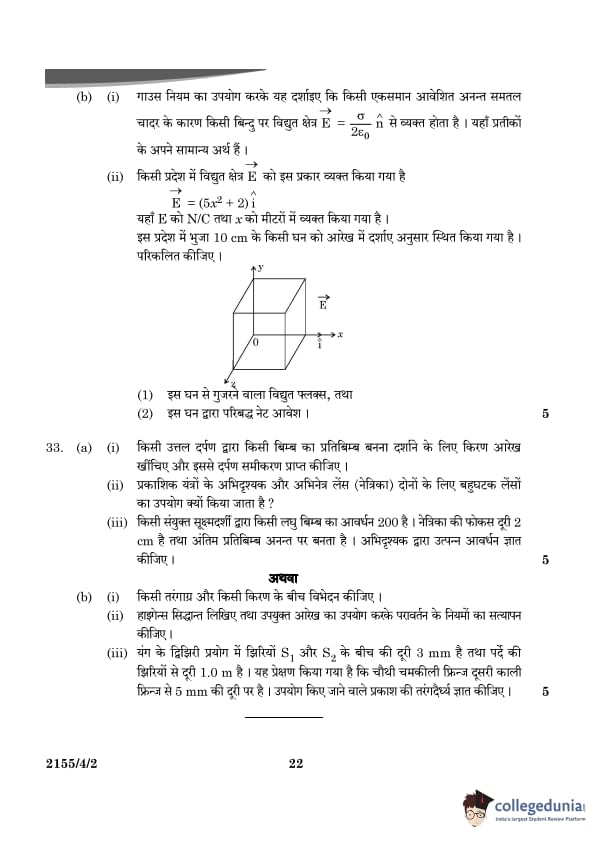
(ii) Electric field \( E \) in a region is given by \( E = (5x^2 + 2) \hat{i} \), where \( E \) is in N/C and \( x \) is in meters. A cube of side 10 cm is placed in the region as shown in the figure. Calculate:
(1) The electric flux through the cube, and
(2) The net charge enclosed by the cube.
View Solution
Flux and Enclosed Charge Calculation
Step 1: Understanding the Given Field
The electric field is:
\[ E = (5x^2 + 2) \hat{i} \]
- The electric field varies with \( x \) but is uniform along the \( y \) and \( z \)-directions.
- The cube has a side length of 10 cm = 0.1 m.
Step 2: Flux Calculation
Electric flux is given by:
\[ \Phi_E = \oint \mathbf{E} \cdot d\mathbf{A} \]
Since the field is in the \( x \)-direction, it only contributes to the flux through the two faces perpendicular to \( x \)-axis.
- At \( x = 0 \) (left face), the field is:
\[ E_{left} = (5(0)^2 + 2) = 2 N/C \]
- At \( x = 0.1 \) m (right face), the field is:
\[ E_{right} = (5(0.1)^2 + 2) = 2 + 5(0.01) = 2.05 N/C \]
Flux through the cube:
\[ \Phi_E = E_{right} A - E_{left} A \]
\[ = (2.05 - 2) (0.1 \times 0.1) \]
\[ = (0.05) (0.01) \]
\[ = 5 \times 10^{-4} Nm^2/C \]
Step 3: Charge Enclosed Using Gauss’s Law
From Gauss’s Law:
\[ \Phi_E = \frac{Q_{enc}}{\epsilon_0} \]
\[ Q_{enc} = \epsilon_0 \Phi_E \]
\[ = (8.85 \times 10^{-12}) (5 \times 10^{-4}) \]
\[ = 4.43 \times 10^{-15} C \]
Thus, the net charge enclosed by the cube is \( 4.43 \times 10^{-15} \) C.
Quick Tip: For a non-uniform field, calculate the flux difference through opposite faces to determine the net charge enclosed.
(i) Draw a ray diagram for the formation of the image of an object by a convex mirror. Hence, obtain the mirror equation.
View Solution
N/A
(ii) Why are multi-component lenses used for both the objective and the eyepiece in optical instruments?
View Solution
N/A
(iii) The magnification of a small object produced by a compound microscope is 200. The focal length of the eyepiece is 2 cm and the final image is formed at infinity. Find the magnification produced by the objective.
View Solution
Magnification Produced by the Objective
Step 1: Total Magnification of Compound Microscope
The total magnification \( M \) produced by the compound microscope is the product of the magnifications of the objective lens (\( M_o \)) and the eyepiece lens (\( M_e \)):
\[ M = M_o \times M_e \]
Given:
- \( M = 200 \) (total magnification),
- The focal length of the eyepiece is \( f_e = 2 cm \).
Step 2: Magnification Produced by the Eyepiece
The magnification produced by the eyepiece is:
\[ M_e = \frac{D}{f_e} \]
where \( D \) is the least distance of distinct vision,
typically taken as 25 cm for a normal human eye.
\[ M_e = \frac{25}{2} = 12.5 \]
Step 3: Magnification Produced by the Objective
Now, using the total magnification:
\[ M = M_o \times M_e \]
\[ 200 = M_o \times 12.5 \]
\[ M_o = \frac{200}{12.5} = 16 \]
Thus, the magnification produced by the objective lens is:
\[ \boxed{M_o = 16} \]
Step 4: Conclusion
The magnification produced by the objective lens is 16.
Quick Tip: In a compound microscope, the total magnification is the product of the magnifications produced by the objective lens and the eyepiece.
(i) Differentiate between a wavefront and a ray.
View Solution
N/A
(ii) State Huygen's principle and verify the laws of reflection using a suitable diagram.
View Solution
N/A
(iii) In Young's double slit experiment, the slits \( S_1 \) and \( S_2 \) are 3 mm apart and the screen is placed 1.0 m away from the slits. It is observed that the fourth bright fringe is at a distance of 5 mm from the second dark fringe. Find the wavelength of light used.
View Solution
We are given the positions of the bright and dark fringes in an interference pattern. The formula used to find the positions is based on the diffraction pattern equations.
For the 4th bright fringe, the position is given by: \[ x_4^{(bright)} = \frac{4\lambda D}{d} \]
where: \( x_4^{(bright)} \) is the position of the 4th bright fringe. \( \lambda \) is the wavelength of light. \( D \) is the distance to the screen. \( d \) is the distance between the slits.
For the 2nd dark fringe, the position is given by: \[ x_2^{(dark)} = \frac{3\lambda D}{2d} \]
where: \( x_2^{(dark)} \) is the position of the 2nd dark fringe.
We are asked to find the difference in positions between the 4th bright fringe and the 2nd dark fringe. Thus, the position difference is: \[ x_4^{(bright)} - x_2^{(dark)} = 5 \, mm \]
Now, we substitute the formulas for the bright and dark fringes: \[ \frac{4\lambda D}{d} - \frac{3\lambda D}{2d} = 5 \times 10^{-3} \, m \]
Simplifying the above equation: \[ \frac{4\lambda D}{d} - \frac{3\lambda D}{2d} = 5 \times 10^{-3} \]
Multiply through by \( d \) to eliminate the denominator: \[ 4\lambda D - \frac{3\lambda D}{2} = 5 \times 10^{-3} d \]
Simplify further: \[ \frac{8\lambda D}{2} - \frac{3\lambda D}{2} = 5 \times 10^{-3} d \] \[ \frac{5\lambda D}{2} = 5 \times 10^{-3} d \]
Finally, solve for \( \lambda \): \[ \lambda = 6 \times 10^{-6} \, m \]
Thus, the wavelength \( \lambda \) of the light is \( 6 \times 10^{-6} \, m \). Quick Tip: In Young’s double slit experiment, the wavelength of light can be calculated using the fringe separation formula, considering the distance between slits and the screen.

Comments