Physics Mentor, VIT Vellore | Updated 3+ months ago
NCERT Solutions for Class 12 Physics Chapter 14 Semiconductor Electronics give step-by-step answers to every back-exercise. Each one is checked against the 2026-27 NCERT and recent CBSE, JEE Main, and NEET papers. This page hosts the full solutions PDF, which you can read or download below.
What Chapter 14 is worth across exams:
CBSE Boards: about 6 marks, usually one 5-mark numerical on rectifier output or the Zener regulator plus a logic-gate truth table.
JEE Main: 3 to 4 percent of the paper, mostly diode circuits, doping levels, and rectifier efficiency.
NEET: 2 to 3 questions each year on n-type vs p-type semiconductors and logic gates.
Why Semiconductor Electronics Matters in Class 12 Physics Chapter 14
Chapter 14 carries 6 board marks, but it counts for even more in entrance exams. Most Modern Physics questions in JEE Main come from semiconductor content, ahead of Chapters 11 to 13. The p-n junction and biasing block is the richest mark cluster, and boards often pair it with a short logic-gate question.
Topic Split for Class 12 Physics Chapter 14 Semiconductor Electronics
The chapter breaks into six blocks. Each one maps to a clear CBSE marking pattern.
Energy bands: 2-mark conceptual on metals, insulators, and semiconductors using band-gap diagrams.
Doping (intrinsic vs extrinsic): 3-mark short answer on what doping is and how it changes conductivity.
n-type and p-type: 2-mark conceptual on donor vs acceptor impurities and majority carriers.
p-n junction and diode: 5-mark derivation block; depletion layer, I-V curves, and diode-as-rectifier carry about 45 percent of the marks.
Rectifiers: 3-mark numerical on half-wave and full-wave output, ripple, and efficiency.
Logic gates: 2 to 3-mark truth-table problems on AND, OR, NOT, NAND, NOR, and XOR.
Exercise Breakdown for Class 12 Physics Chapter 14 NCERT Solutions
The chapter has 12 back exercises plus 7 solved examples. Exercises 14.1 to 14.4 are conceptual on band theory and doping. Exercises 14.5 to 14.12 are multi-step numericals on p-n junction circuits, rectifier efficiency, and logic gates.
Exercise / Section
Questions
Sub-topic Focus
Example 14.1 to 14.7
7 in-text
Band theory, doping, p-n junction, rectifier, logic gates
Exercise 14.1 to 14.4
4
Energy bands, intrinsic vs extrinsic semiconductors
Exercise 14.5 to 14.8
4
p-n junction, diode I-V curve, forward and reverse bias
Exercise 14.9 to 14.12
4
Rectifier, Zener regulator, logic gates
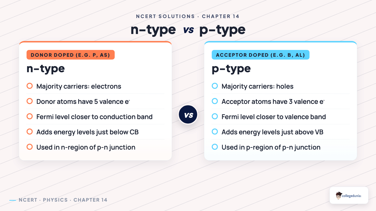
n-type vs p-type semiconductors at a glance.
Intrinsic vs Extrinsic and N-Type vs P-Type Semiconductor Class 12
Intrinsic semiconductors are pure, so electron and hole counts are equal and depend only on temperature. Extrinsic semiconductors are doped, so one carrier type becomes the majority and the doping level sets the conductivity. This pair is a common 2 to 3-mark CBSE question.
n-type uses pentavalent donors, so electrons are the majority carrier and the Fermi level sits near the conduction band. p-type uses trivalent acceptors, so holes are the majority carrier and the Fermi level sits near the valence band. Both stay electrically neutral overall, because the fixed impurity ions balance the moving carriers.
Energy Bands, Doping, and Devices in Semiconductor Electronics Class 12
In a solid, atomic levels merge into a filled valence band and an empty conduction band. Metals have overlapping bands, so they conduct freely. Insulators have a large gap above 3 eV. Semiconductors have a small gap (about 1.1 eV for Si, 0.7 eV for Ge), so heat lifts a few electrons across and gives partial conduction.
Doping adds a tiny amount of impurity, often 1 atom per million, but it raises conductivity by a huge factor. Pentavalent donors such as phosphorus give extra electrons, while trivalent acceptors such as boron leave holes.
The main devices in this chapter are the p-n junction diode, the Zener diode as a voltage regulator, half-wave and full-wave rectifiers, and the logic gates. Boards also rotate the photodiode, the LED, and the solar cell as 2-mark short answers, and the PDF covers all of them.
Semiconductor Electronics Class 12 Formula Quick-Reference
These 12 formulas cover every numerical in Chapter 14.
Concept
Formula
SI Unit
Mass-action law (intrinsic)
n times p = n_i squared
per m^6
Conductivity
sigma = e (n mu_e + p mu_h)
S/m
Diode current (Shockley)
I = I_0 (exp(eV/kT) minus 1)
ampere
Half-wave DC voltage
V_dc = V_max / pi
volt
Half-wave efficiency
eta = 40.6%
percent
Full-wave DC voltage
V_dc = 2 V_max / pi
volt
Full-wave efficiency
eta = 81.2%
percent
Ripple factor (half-wave)
r = 1.21
dimensionless
Ripple factor (full-wave)
r = 0.48
dimensionless
Zener regulator
V_out = V_Z (constant)
volt
NAND
NAND = NOT(AND)
n/a
NOR
NOR = NOT(OR)
n/a
Semiconductor Electronics Weightage Across Class 12 Physics Chapters
The table below shows how Chapter 14 compares with other Class 12 Physics chapters. At 6 marks it ties with Chapters 1, 4, and 7 among the heavy-weight chapters.
Chapter
Topic
Avg CBSE Marks
Ch 1
Electric Charges and Fields
6 marks
Ch 2
Electrostatic Potential and Capacitance
7 marks
Ch 3
Current Electricity
7 marks
Ch 4
Moving Charges and Magnetism
6 marks
Ch 7
Alternating Current
6 marks
Ch 9
Ray Optics and Optical Instruments
7 marks
Ch 11
Dual Nature of Radiation and Matter
4 marks
Ch 13
Nuclei
3 marks
Ch 14
Semiconductor Electronics
6 marks
NCERT Solutions for Class 12 Physics: All Chapters
The table below lists every Class 12 Physics NCERT Solutions page in chapter order.
All NCERT Solutions for Class 12 Physics Chapter 14 Semiconductor Electronics with Step-by-Step Solutions
Every question of NCERT Class 12 Physics Semiconductor Electronics is listed below with its full Solution and Expert Solution hidden inside collapsible tabs. Click Check Solution to reveal the step-by-step working; click Expert Solution for the expanded explanation.
Q 14.1
In an n-type silicon, which of the following statement is true:
(a) Electrons are majority carriers and trivalent atoms are the dopants.
(b) Electrons are minority carriers and pentavalent atoms are the dopants.
(c) Holes are minority carriers and pentavalent atoms are the dopants.
(d) Holes are majority carriers and trivalent atoms are the dopants.
What the question is asking. We have to pick the correct statement describing the carrier population and the dopant type used to make n-type silicon. The word "n" already tells us something - let's decode it carefully.
Given.
Host crystal: silicon (group IV, four valence electrons).
Doping type: n-type.
Concept used - extrinsic semiconductors. Silicon is a pure (intrinsic) semiconductor with four valence electrons per atom. If we add a tiny amount of an impurity (this is called doping), we change its conduction behaviour dramatically.
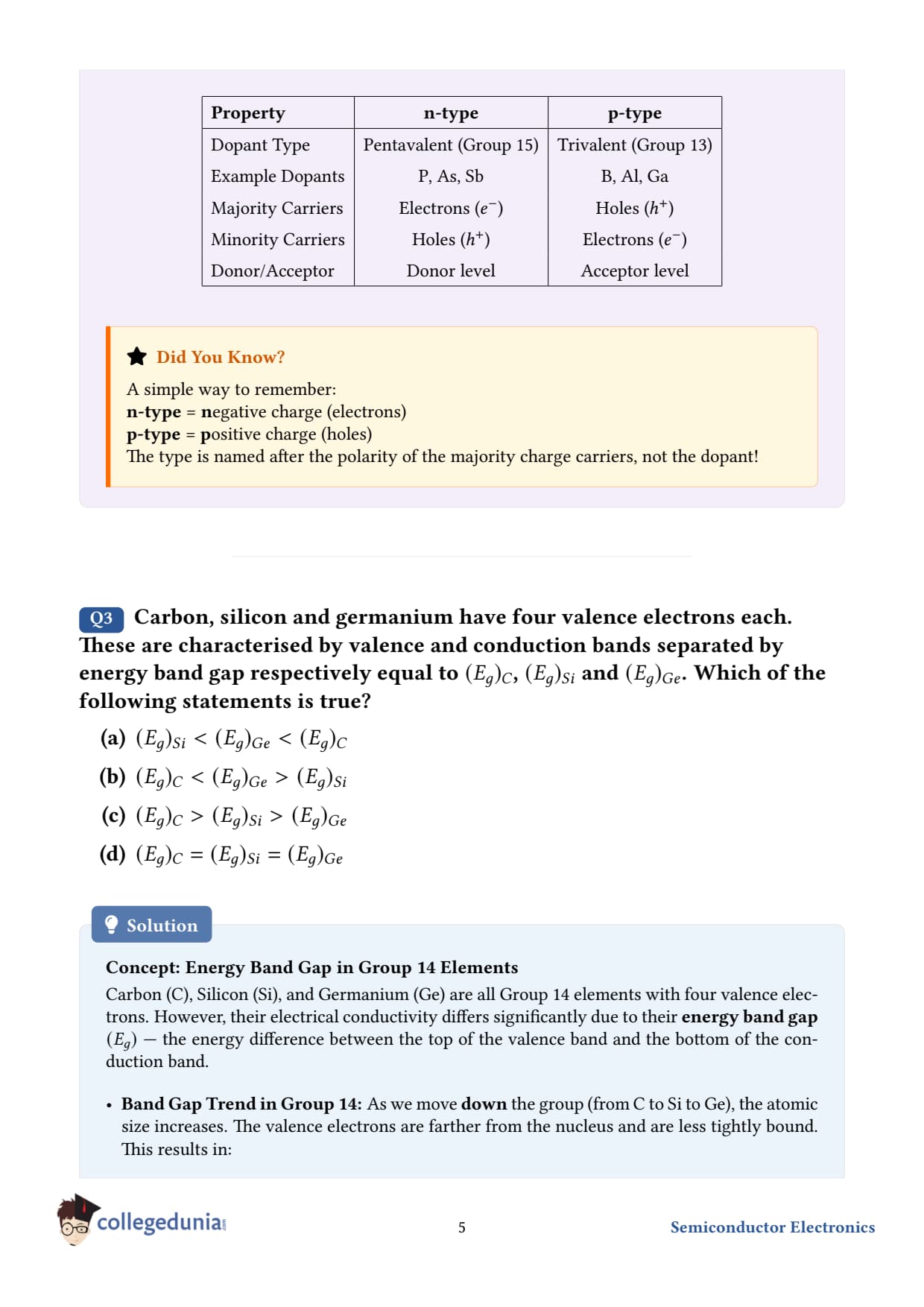
n-type: dope with a pentavalent atom (5 valence electrons - P, As, Sb). Four of the five electrons form covalent bonds with neighbouring Si atoms; the fifth is loosely bound and easily becomes a free conduction electron. Electrons therefore become majority carriers; holes are minority carriers. The "n" stands for negative (the sign of the majority carrier charge).
p-type: dope with a trivalent atom (3 valence electrons - B, Al, In, Ga). It is one electron short of a full bond → leaves a hole. Holes are majority carriers; electrons are minority.
Step 1 - identify majority carriers in n-type. Electrons. ✓
Step 2 - identify the dopant. Pentavalent atom (P, As, Sb). ✓
Step 3 - identify minority carriers. Holes.
Step 4 - scan the options.
(a) Electrons majority ✓, but trivalent dopant ✗ → wrong.
Final answer. Option (c) - holes are minority carriers and pentavalent atoms are the dopants.
DR
Dr. Rajesh Kumar
Ph.D. Physics, IIT Delhi
Verified Expert
Numbers that matter. In intrinsic Si at room temperature the carrier density is ni ≈ 1.51016 m-3. With a typical donor doping of 1022 m-3, the electron density jumps by a factor of about 106. Holes, by the law of mass action ne nh = ni2, drop to about 21010 m-3 - six orders of magnitude less than the electrons. That huge asymmetry is the whole basis of "majority vs minority" carriers.
Energy-band picture. A pentavalent donor introduces a discrete energy level just below the conduction band donor level, ∼ 0.05 eV below Ec for P in Si. At room temperature this small gap is easily bridged by thermal energy kT ≈ 0.025 eV, so essentially every donor atom is ionised and contributes one free electron.
Common mistake. "n-type" does NOT mean the crystal is negatively charged! The crystal as a whole stays electrically neutral - the donor ion left behind after losing its fifth electron carries a +1 charge that exactly balances the freed electron. The "n" only labels the sign of the majority mobile carrier.
Real world. Almost every chip you own - CPUs, memory, image sensors - is built from precisely engineered n- and p-type regions on a silicon wafer. Modern doping can place donor atoms with atomic-scale accuracy using ion implantation.
Q 14.2
Which of the statements given in Exercise 14.1 is true for p-type semiconductors.
What the question is asking. Same four statements as Q14.1, but now for p-type silicon. Find the one that is correct.
Concept used. A p-type semiconductor is created by doping intrinsic Si with a trivalent impurity such as B, Al, In, Ga (group III, three valence electrons). The impurity creates a "missing" covalent bond - a vacant site that behaves like a positively charged particle called a hole.
Majority carriers: holes.
Minority carriers: electrons.
Dopant: trivalent atom.
Step 1 - write what must be true for p-type. Holes majority, electrons minority, trivalent dopant.
Step 2 - scan the four options.
(a) Electrons majority ✗.
(b) Electrons minority ✓ AND pentavalent dopant ✗ → wrong.
(c) Holes minority ✗.
(d) Holes majority ✓ AND trivalent dopant ✓ → CORRECT.
Final answer. Option (d) - holes are majority carriers and trivalent atoms are the dopants.
DA
Dr. Anjali Verma
Ph.D. Physics, IIT Bombay
Verified Expert
What is a "hole"? A hole is not a real particle - it is the absence of an electron in an otherwise filled covalent bond. When a neighbouring electron jumps into that vacancy, the vacancy itself appears to move in the opposite direction. We track it as if it were a positive particle of charge +e and effective mass slightly larger than the electron's.
Acceptor level. A trivalent dopant introduces an empty energy level just above the valence band (acceptor level). Thermal energy easily promotes electrons from the valence band into this level, leaving holes behind in the valence band.
Common mistake. "p-type" does NOT mean the crystal is positively charged. After accepting an electron, the dopant atom becomes a stationary negative ion that balances the mobile hole's charge. The crystal stays neutral overall.
Why we need both types. Modern semiconductor devices (diodes, BJTs, MOSFETs, solar cells, LEDs) all rely on bringing p-type and n-type regions into contact. The p–n junction is the building block of almost all modern electronics.
Q 14.3
Carbon, silicon and germanium have four valence electrons each. These are characterised by valence and conduction bands separated by energy band gap respectively equal to EgC, EgSi and EgGe. Which of the following statements is true?
(a) EgSi < EgGe < EgC
(b) EgC < EgGe > EgSi
(c) EgC > EgSi > EgGe
(d) EgC = EgSi = EgGe
What the question is asking. Three group-IV elements - diamond (C), silicon (Si), germanium (Ge) - all have four valence electrons. Order their band gaps.
Concept used - band gap and atomic size. The band gap Eg is the energy a valence electron must absorb to reach the conduction band and become a free carrier.
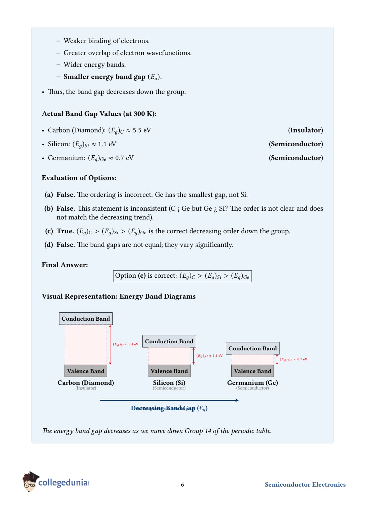
As we go down group IV from C → Si → Ge, the atoms get bigger:
Atomic radius of C ≈ 0.077 nm, Si ≈ 0.118 nm, Ge ≈ 0.122 nm.
Larger atoms → weaker bonding between valence electrons and the nucleus → easier to free → smaller band gap.
Standard numerical values.
EgC (diamond) ≈ 5.4 eV → INSULATOR.
EgSi ≈ 1.1 eV → semiconductor.
EgGe ≈ 0.7 eV → narrow-gap semiconductor.
Step 1 - order them.5.4 > 1.1 > 0.7, so EgC > EgSi > EgGe.
Step 2 - pick the matching option. That is option (c).
Final answer. Option (c) - (Eg)C > (Eg)Si > (Eg)Ge.
DS
Dr. Sneha Iyer
Ph.D. Physics, IISc Bangalore
Verified Expert
Why band gap shrinks down a group. Moving down group IV, two effects compound: (i) the lattice constant increases, so the overlap between neighbouring atomic orbitals decreases; (ii) outer valence electrons are screened by more inner shells, weakening their hold on the nucleus. Both push the conduction-band minimum closer to the valence-band maximum.
Conductor vs insulator vs semiconductor in band language.
Conductor: conduction band partly filled OR overlaps with the valence band Eg = 0. Examples - Cu, Al.
Insulator: Eg 3 eV. Almost no electrons get thermally excited. Examples - diamond, glass.
Semiconductor: Eg ≈ 0.2–2 eV. A useful fraction of carriers is thermally excited at room temperature and can be controlled by doping.
Alternate route - Mott's rule of thumb. Optical absorption edge gives Eg. Diamond is transparent right through visible because Eg = 5.4 eV ≫ visible photon energies of 1.6–3.2 eV; Si is opaque to visible light but transparent to infrared because Eg = 1.1 eV corresponds to wavelength ∼ 1100 nm; Ge is transparent to slightly longer IR.
Real world. Si dominates because its band gap is "just right" for room-temperature electronics and it has a tough oxide (SiO₂) for insulation. Ge transistors were used in the 1950s but lost out because of higher leakage. Diamond is being researched as a high-power, high-temperature semiconductor.
Q 14.4
In an unbiased p-n junction, holes diffuse from the p-region to n-region because
(a) free electrons in the n-region attract them.
(b) they move across the junction by the potential difference.
(c) hole concentration in p-region is more as compared to n-region.
(d) All the above.
What the question is asking. Why do holes diffuse from p-side to n-side in an unbiased p–n junction?
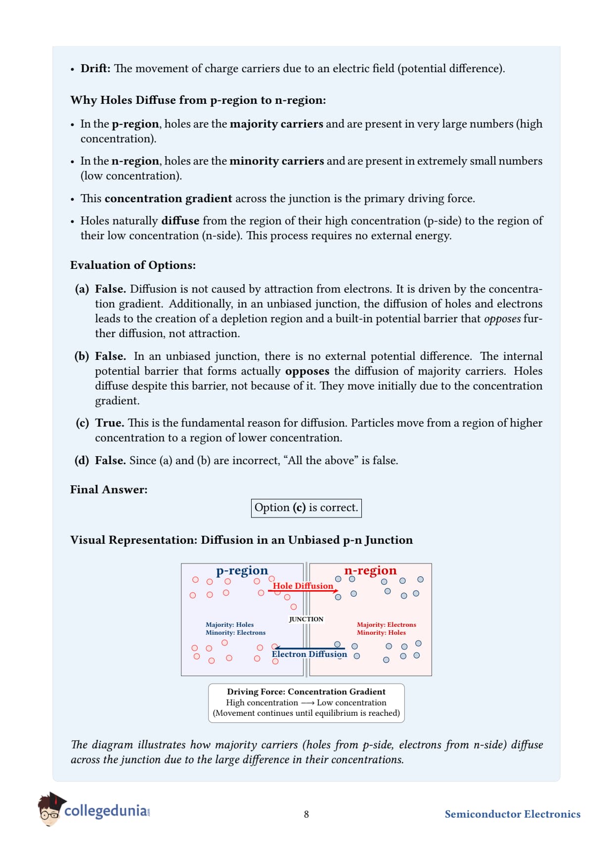
Concept used - diffusion. Diffusion is the net motion of particles from a region of HIGH concentration to a region of LOW concentration. It is driven purely by the concentration gradient (statistics), not by any external attraction or applied field. The mathematical statement is Fick's law: Jdiff = -Ddndx, where D is the diffusion coefficient.
Step 1 - compare hole concentrations across the junction.
p-side: holes are MAJORITY carriers → very high hole concentration.
n-side: holes are MINORITY carriers → very low hole concentration.
Step 2 - apply Fick's law. The gradient pushes holes from p (high) to n (low). This diffusion happens BEFORE any electric field has had a chance to build up - that is, at the moment the junction is first formed.
Step 3 - check the other options.
(a) Electrons attracting holes? Coulomb attraction is too weak in a neutral crystal - and holes/electrons inside the bulk don't pair up like that. Wrong.
(b) Potential difference driving diffusion? Confused - in an unbiased junction, the barrier potential opposes further hole diffusion (it's set up by the diffusion!). Wrong direction of cause and effect.
Final answer. Option (c) - hole concentration in the p-region is greater than in the n-region.
DV
Dr. Vivek Sharma
Ph.D. Physics, Delhi University
Verified Expert
The depletion-layer story. When p and n regions are joined, diffusion immediately moves holes p → n and electrons n → p. As soon as a hole crosses, it leaves behind a stationary negative acceptor ion on the p-side; the electron leaves behind a stationary positive donor ion on the n-side. Together, the immobile ions form a depleted region with a built-in electric field pointing from n to p. This field opposes further diffusion. Equilibrium is reached when the diffusion current is exactly cancelled by the drift current driven by the built-in field.
Built-in potential. For Si at room temperature with typical doping the built-in potential is about V0 = kTe ln(NA NDni2) ≈ 0.7 V. This is the "potential barrier" referred to in textbooks.
Common mistake. Don't confuse diffusion (statistical, due to gradient) with drift (electrical, due to field). Diffusion needs no field; drift needs a field. Both currents exist in a p–n junction and balance at equilibrium.
Real world. Every solar cell exploits this: light creates extra electron-hole pairs near the junction, the built-in field separates them, and the resulting current flows through the load.
Q 14.5
When a forward bias is applied to a p-n junction, it
(a) raises the potential barrier.
(b) reduces the majority carrier current to zero.
(c) lowers the potential barrier.
(d) None of the above.
What the question is asking. What does forward bias do to the built-in barrier of a p–n junction?
Concept used - forward bias. Forward bias means the p-side is connected to the positive terminal of the battery and the n-side to the negative terminal.
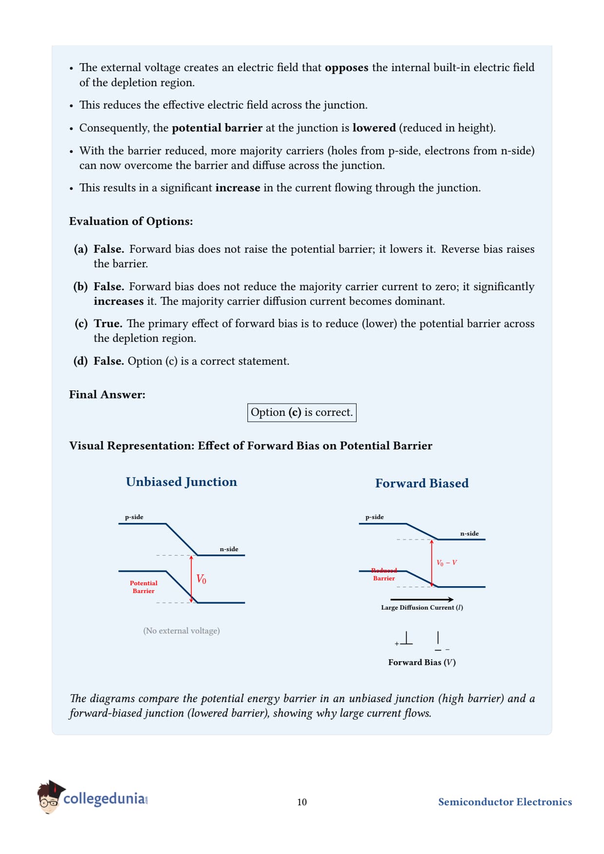
The applied voltage is in the OPPOSITE direction to the built-in field.
Net potential across the junction = V0 - V (built-in minus applied).
So the barrier height decreases.
Step 1 - recall the geometry. The built-in field points from n to p (because positive ions sit on the n-side, negative ions on the p-side). Forward bias applies a field in the opposite direction (from p to n inside the external circuit pushes positive charge into the p-side).
Step 2 - picture the energy diagram. Before bias, an energy "hill" of height eV0 ≈ 0.7 eV separates holes in the p-side from holes in the n-side (and similarly for electrons). Forward bias lowers this hill by eV.
Step 3 - consequence for current. With a lower barrier, many more majority carriers can climb over it: holes pour from p to n, electrons from n to p. Current rises rapidly (exponentially) with the applied voltage. The diode is "on".
Step 4 - evaluate options.
(a) Raises the barrier? No - that's reverse bias. Wrong.
(b) Majority current zero? No - it INCREASES. Wrong.
(c) Lowers the barrier. CORRECT.
Final answer. Option (c) - forward bias lowers the potential barrier.
DS
Dr. Shalini Menon
M.Sc Physics, University of Hyderabad
Verified Expert
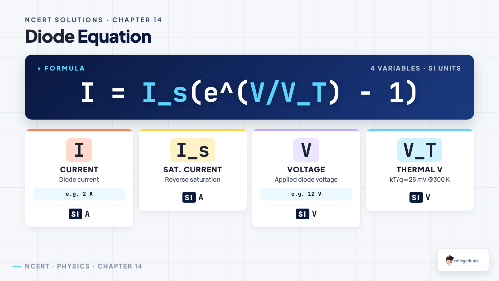
The diode equation. The full current–voltage relation for an ideal diode is I = I0(eeV/kT - 1), where I0 is the reverse saturation current and V is positive for forward bias, negative for reverse. The exponential dependence on V is what makes diodes such sharp switches: changing V by just 0.06 V at room temperature changes the current by a factor of 10.
Why the barrier shrinks. The applied potential V drops almost entirely across the high-resistance depletion region (the bulk Si has low resistance), so the depletion region itself becomes thinner and the energy step across it shrinks from eV0 to eV0 - V.
Common mistake. Forward bias does NOT make minority-carrier flow stop - minority carriers still drift the other way as before. What forward bias does is unleash the much larger majority-carrier current. The net current is overwhelmingly the majority diffusion current.
Real world. The "turn-on" voltage of a Si diode ∼ 0.7 V and of an LED ∼ 2–3.5 V depending on colour is set by the band gap of the semiconductor used.
Q 14.6
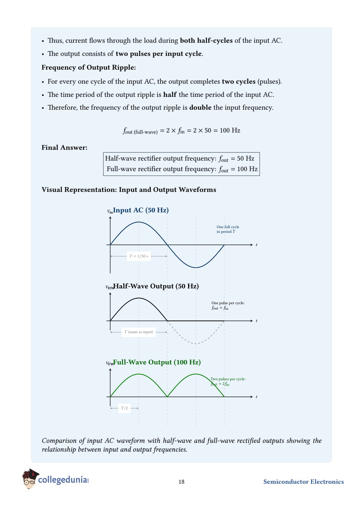
In half-wave rectification, what is the output frequency if the input frequency is 50 Hz. What is the output frequency of a full-wave rectifier for the same input frequency.
What the question is asking. Find the output (ripple) frequency for a half-wave and a full-wave rectifier when fed a 50 Hz AC mains supply.
Given.
Input AC frequency, fin = 50 Hz.
Concept used - rectification.
Half-wave rectifier: uses a single diode. It conducts during ONLY the positive half-cycles of the input; the negative half is blocked. So the output is a series of pulses, one per input cycle.
Full-wave rectifier: uses two diodes (or a bridge of four). The negative half-cycle is also flipped to positive, so the output has TWO positive pulses per input cycle.
Step 1 - half-wave output frequency. Each input cycle produces one output pulse, so fout, HW = fin = 50 Hz.
Step 2 - full-wave output frequency. Each input cycle produces two output pulses, so fout, FW = 2 fin = 2× 50 = 100 Hz.
Final answer. fout, HW = 50 Hz, fout, FW = 100 Hz.
DR
Dr. Rajesh Kumar
Ph.D. Physics, IIT Delhi
Verified Expert
Why "frequency" of a rectified signal is well-defined. The output isn't a sine wave but a periodic train of pulses; its fundamental frequency is the inverse of the time between successive pulses. For HW that interval equals the input period T; for FW it equals T/2.
Smoothing. Adding a capacitor (or LC) filter across the rectifier output smooths the pulses into a near-DC voltage with small "ripple". The ripple frequency equals the output pulse frequency - 50 Hz for HW, 100 Hz for FW. Full-wave is preferred in power supplies because:
The filter capacitor recharges twice as often → smaller voltage droop.
Better transformer utilisation.
Higher DC content V= 2Vm/π vs Vm/π.
Common mistake. Students sometimes write "frequency = 0 because it's DC". The output is "pulsating DC" - its average is DC, but it still has an AC ripple component at the rectification frequency.
Real world. Your laptop charger uses a bridge rectifier followed by a filter and a switching regulator - the 100 Hz ripple is exactly what the bulky capacitor inside the brick is fighting.
Q 14.7
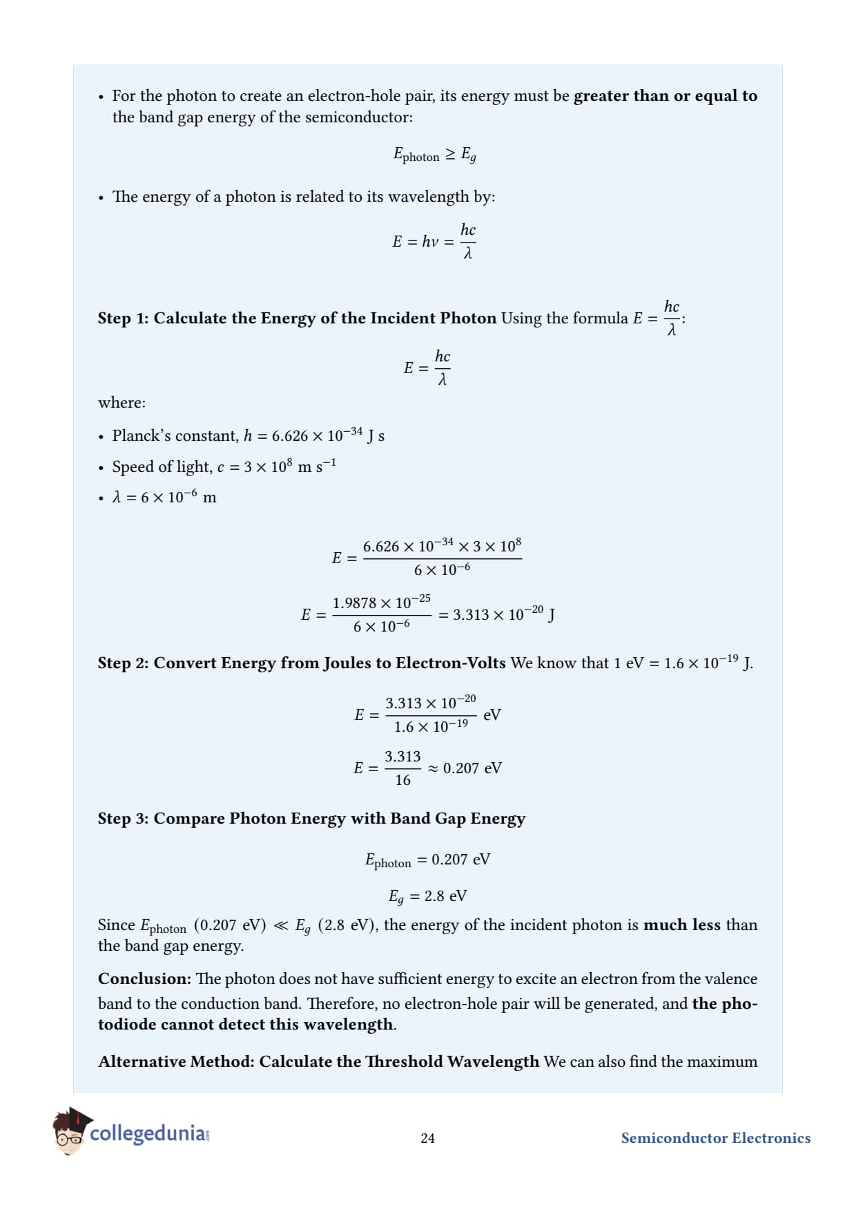
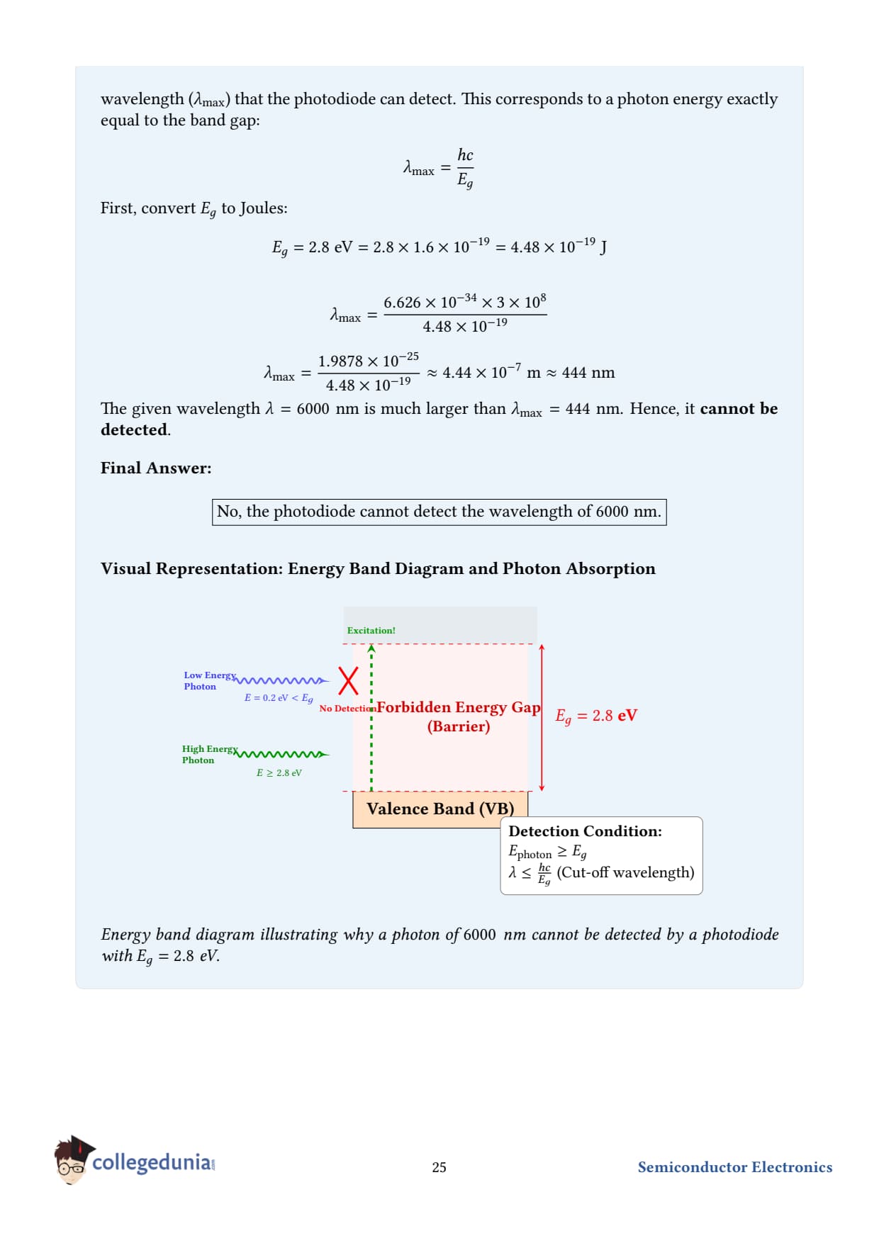
A p-n photodiode is fabricated from a semiconductor with band gap of 2.8 eV. Can it detect a wavelength of 6000 nm?
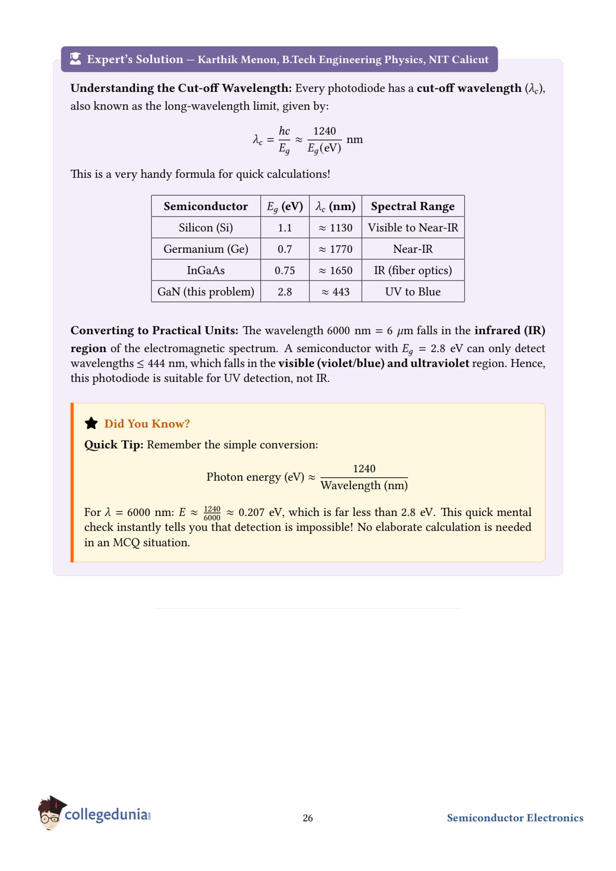
What the question is asking. A photodiode generates electron–hole pairs only when the incoming photon energy is at least equal to the band gap. We must check whether 6000 nm photons have enough energy.
Given.
Band gap, Eg = 2.8 eV.
Wavelength, λ = 6000 nm = 610-6m.
Concept used - photon energy. Ephoton = hcλ, where h = 6.6310-34Js, c = 3108m/s. A handy shortcut in eV and nm: Ephoton(eV) = 1240λ(nm). For the photodiode to detect light, Ephoton ≥ Eg.
Step 1 - write the formula. Ephoton = 1240λ(nm) eV.
Step 3 - compare with band gap. Ephoton = 0.207 eV < Eg = 2.8 eV.
Step 4 - verdict. The photon does NOT carry enough energy to lift an electron from the valence to the conduction band, so no electron–hole pair is created and no photocurrent flows.
Final answer. No - the photodiode cannot detect (6000 nm) light because the photon energy 0.207 eV is much smaller than the band gap 2.8 eV.
DA
Dr. Anjali Verma
Ph.D. Physics, IIT Bombay
Verified Expert
Cut-off wavelength. The longest wavelength the diode can detect is c = hcEg = 12402.8 nm ≈ 443 nm. This sits in the violet-blue region of the visible spectrum. Anything redder than 443 nm - including the infrared 6000 nm given in the problem - is invisible to this diode.
Choosing a photodiode. Material selection is dictated by the target wavelength:
UV/blue: GaN, SiC.
Visible: Si Eg = 1.1 eV, c ≈ 1100 nm.
Near-IR 1.55 fibre telecom: InGaAs.
Mid-IR (3–14 µm thermal imaging): HgCdTe.
Common mistake. Don't read 6000 nm as 600 nm - the former is mid-IR, the latter is orange visible. A factor of 10 in wavelength changes the photon energy by a factor of 10, which can completely change the answer.
Real world. The same logic explains why Si solar cells lose all sub-1100 nm IR photons - they pass right through. Multi-junction cells stack different-bandgap materials to capture more of the spectrum.
Q 14.8
The number of silicon atoms per m3 is 51028. This is doped simultaneously with 51022 atoms per m3 of Arsenic and 51020 per m3 atoms of Indium. Calculate the number of electrons and holes. Given that ni = 1.51016 m-3. Is the material n-type or p-type?
What the question is asking. A Si sample is doped with BOTH a donor (As) and an acceptor (In). The two partially cancel. Find the resulting electron concentration ne and hole concentration nh and identify the type.
Given.
Donor (As, pentavalent) density, ND = 51022 m-3.
Acceptor (In, trivalent) density, NA = 51020 m-3.
Intrinsic carrier density, ni = 1.51016 m-3.
Concept used.
Net donor density when both are present: ND - NA. The smaller acceptor population just removes some of the donor electrons.
For heavy doping ND - NA ≫ ni the electron density is essentially equal to the net donor density: ne ≈ ND - NA.
Law of mass action:ne nh = ni2. This is a thermodynamic equilibrium relation valid for any non-degenerate semiconductor.
Step 1 - net donor density. ND - NA = 51022 - 51020 = 51022 - 0.051022 = 4.951022 m-3.
Step 2 - electron density. Since ND - NA ≫ ni, ne ≈ 4.951022 m-3.
Step 3 - hole density from mass action. nh = ni2ne = (1.51016)24.951022 = 2.2510324.951022.
Step 5 - identify type. Electrons ∼ 51022 dominate holes ∼ 5109 by 13 orders of magnitude → this is an n-type semiconductor.
Final answer. ne ≈ 4.951022 m-3, nh ≈ 4.5109 m-3, n-type.
DV
Dr. Vivek Sharma
Ph.D. Physics, Delhi University
Verified Expert
Compensation doping. When both donors and acceptors are present, they "compensate" each other. The net result is determined by whichever dopant has the higher density. Compensation is intentionally used in real chips to fine-tune carrier concentrations: you can over-dope p-type, then back-compensate with donors to land exactly on a target carrier density.
Why ne ≈ ND - NA and not exactly equal. Charge neutrality demands ne + NA- = nh + ND+. Combined with the mass action law ne nh = ni2, this gives the exact quadratic. For our numbers the corrections from nh and incomplete ionisation are utterly negligible (parts per trillion).
Common mistake. Forgetting the law of mass action and computing nh directly from NA. NA is the acceptor density, not the hole density. In a heavily n-doped sample most acceptors capture electrons from the donor pool and never produce free holes.
Real world. A 13-order-of-magnitude carrier asymmetry is what makes diodes such efficient one-way valves. The reverse saturation current is set by the tiny minority population - about 109 m-3 here - making leakage in reverse bias minuscule.
Q 14.9
In an intrinsic semiconductor the energy gap Eg is 1.2 eV. Its hole mobility is much smaller than electron mobility and independent of temperature. What is the ratio between conductivity at 600 K and that at 300 K? Assume that the temperature dependence of intrinsic carrier concentration ni is given by ni = n0 exp(-Eg2kBT), where n0 is a constant.
What the question is asking. Find 600 K/300 K for an intrinsic semiconductor with band gap 1.2 eV, given the standard exponential form for ni(T).
Given.
Eg = 1.2 eV.
Hole mobility h ≪ electron mobility e, both independent of temperature.
ni = n0 e-Eg/2kBT.
Boltzmann constant kB = 8.6210-5 eV/K.
Concept used - conductivity of an intrinsic semiconductor. σ = nie (e + h) ≈ niee (since h ≪ e). With e temperature-independent, the ratio of conductivities equals the ratio of carrier concentrations: 21 = ni(T2)ni(T1) = expEg2kB(1T1 - 1T2).
Final answer.600 K300 K ≈ 1.1× 10⁵. The conductivity rises by roughly five orders of magnitude when the temperature is doubled.
DS
Dr. Sneha Iyer
Ph.D. Physics, IISc Bangalore
Verified Expert
Why the factor of 2 in the exponent. Both electrons and holes are created in equal numbers from band-to-band excitation: ne = nh = ni. The probability of an electron jumping from the valence band to the conduction band depends on exp-Eg/kBT, but ni ∝ √Nc Nv exp(-Eg/2kBT) by the law of mass action. That is the origin of the 2kBT - each carrier "owes" half of the gap energy.
Alternative method - Arrhenius plot. Plot ln σ versus 1/T on a log–linear scale. The slope is -Eg/2kB; this is the standard experimental way to extract a semiconductor's band gap.
Common mistake. Forgetting the factor of 2: writing σ ∝ exp-Eg/kBT gives an exponent twice as large and a ratio of ∼ 1010 - wildly off.
Real world. This dramatic temperature sensitivity is exactly why semiconductors make excellent thermistors and why your phone slows down when it gets hot. It's also why early Ge transistors Eg = 0.7 eV needed heat sinks - even a small temperature rise made the minority current explode.
Q 14.10
In a p-n junction diode, the current I can be expressed as I = I0 exp(eV2kBT) - 1, where I0 is called the reverse saturation current, V is the voltage across the diode and is positive for forward bias and negative for reverse bias, and I is the current through the diode, kB is the Boltzmann constant 8.6× 10⁻⁵ eV/K and T is the absolute temperature. If for a given diode I0 = 510-12A and T = 300 K, then
(a) What will be the forward current at a forward voltage of 0.6 V?
(b) What will be the increase in the current if the voltage across the diode is increased to 0.7 V?
(c) What is the dynamic resistance?
(d) What will be the current if reverse bias voltage changes from 1 V to 2 V?
Given.
I0 = 510-12A.
T = 300 K.
kB = 8.610-5 eV/K.
Thermal voltage at T: kBTe = 8.610-5× 300 = 0.0258 V. Hence eV2kBT = V2× 0.0258 = V0.0516.
(c) Dynamic resistance between these two operating points. rd = Δ VΔ I = 0.1 V3.3410-6A ≈ 3.0104 Ω = 30 kΩ.
(d) Current when reverse bias changes from -1 V to -2 V.
For V ≪ 0, eeV/2kBT → 0, so I → -I0 = -5× 10-12A. The current is essentially the reverse saturation current, INDEPENDENT of the magnitude of the reverse voltage. Therefore the change in current is ≈ 0.
Final answers. (a) I ≈ 0.55 ; (b) Δ I ≈ 3.34 ; (c) rd ≈ 30 kΩ; (d) Δ I ≈ 0.
DR
Dr. Rajesh Kumar
Ph.D. Physics, IIT Delhi
Verified Expert
The "ideality factor". The exercise uses eV/2kBT, corresponding to an ideality factor n = 2 typical of Si diodes where recombination in the depletion region dominates. The textbook ideal diode (Shockley) uses n = 1. Real Si diodes lie in between depending on the bias regime.
Why current rises ~10× per 0.06 V change. Because eV/0.0516 = e(V+0.06)/0.0516/e0.06/0.0516 = e0.06/0.0516 old ≈ 3.2×. With n=1VT = 0.026 the factor is e0.06/0.026 ≈ 10 per 60 mV - the famous "decade per 60 mV" rule.
Why reverse current saturates. Reverse bias starves the majority-carrier diffusion almost completely; only the few minority carriers generated thermally close to the junction are swept across by the field. Their supply is set by temperature, not by voltage.
Real world. Dynamic resistance of 30 kΩ is huge - but it drops sharply at higher currents. At I = 1 mA, rd ≈ 2kBT/(eI) ≈ 50 Ω. That's why diodes are good logarithmic compressors and why the same diode can be used to build temperature sensors.
Q 14.11
You are given the two circuits as shown in Fig. 14.36. Show that circuit (a) acts as OR gate while the circuit (b) acts as AND gate.
What the question is asking. Fig. 14.36 shows two combinations of basic logic gates. We have to identify what overall function each implements by writing out its truth table.
Concept used - building gates from NAND/NOR.
Circuit (a): two inputs A, B are first fed to two NOT gates; the two NOT outputs are fed to a NAND gate. Equivalent expression: Y = A·B̄ = A + B (De Morgan). This is the OR function.
Circuit (b): A and B feed a NAND gate; the NAND output passes through a NOT gate. Expression: Y = A· B̄̄ = A· B. This is the AND function.
Step 1 - verify circuit (a) by truth table.
A
B
A
B
A · B
Y = A · B̄
0
0
1
1
1
0
0
1
1
0
0
1
1
0
0
1
0
1
1
1
0
0
0
1
Column Y matches the OR truth table.
Step 2 - verify circuit (b) by truth table.
A
B
A· B
NAND =A· B̄
Y=A· B̄̄
0
0
0
1
0
0
1
0
1
0
1
0
0
1
0
1
1
1
0
1
Column Y matches the AND truth table.
Final answer. Circuit (a) = OR gate, Circuit (b) = AND gate.
DA
Dr. Anjali Verma
Ph.D. Physics, IIT Bombay
Verified Expert
De Morgan's theorems - the bedrock.A· B̄ = A + B, A + B̄ = A · B. Any logic function whatsoever can be built using only NAND gates or only NOR gates - they are called universal gates. The two circuits in the question are textbook examples of this universality.
Alternative implementation. The AND function in circuit (b) could equally be obtained from two NOR gates via A + B̄ = A· B. The OR function in circuit (a) could be built from two NOR gates by A+B̄̄ = A+B. Try drawing those circuits - they help cement De Morgan.
Common mistake. Confusing the bar levels. Write the expression at each node carefully before applying De Morgan; never apply both bars and a flip simultaneously.
Real world. Inside any CPU, billions of transistors are wired into NAND/NOR cells. The fabrication process is most efficient when only one universal gate type is used; this is why CMOS chips often look like a sea of NAND gates. The OR and AND we use in code reduce, at the silicon level, to constructions exactly like (a) and (b).
Q 14.12
Write the truth table for a NAND gate connected as given in Fig. 14.37. Hence identify the exact logic operation carried out by this circuit.
What the question is asking. In Fig. 14.37 a NAND gate has BOTH its inputs tied together to a single line A. We must write the truth table and name the operation.
Concept used. The NAND output is A· B̄. If both inputs are tied to A then B = A, so Y = A· Ā = Ā = NOT A.
Step 1 - write the truth table.
A = B
A· B
Y = A· B̄
0
0
1
1
1
0
Step 2 - identify operation. Output equals 1 when input is 0 and 0 when input is 1 - this is the NOT (inverter) operation.
Final answer. The circuit acts as a NOT gate (inverter): Y = A.
DV
Dr. Vivek Sharma
Ph.D. Physics, Delhi University
Verified Expert
Why this trick matters. Among all the basic gates, NAND (and NOR) are the only ones from which every other gate can be built. The very first step in that construction is exactly this one - turn a NAND into a NOT by shorting its inputs. From a NOT and a NAND you can build AND (next problem), and from AND and NOT you can build everything.
Boolean identities at work.A· A = A (idempotent law), Ā = 1 - A. Combined: A· Ā = Ā.
Common mistake. Don't read the diagram as "two independent inputs both set to A" and assume Y is computed by feeding two different probability values. The two inputs are physically the same wire - they cannot disagree.
Real world. In a 7400 series IC, a single quad-NAND chip (7400) can be reconfigured: with input pins shorted in pairs, each NAND becomes a NOT, giving four inverters in one package. Cost-conscious 1970s designers used this trick to avoid stocking a separate 7404 inverter chip.
Q 14.13
You are given two circuits as shown in Fig. 14.38, which consist of NAND gates. Identify the logic operation carried out by the two circuits.
What the question is asking. Both circuits are made entirely of NAND gates. Identify the function each performs.
Circuit (a) - two NAND followed by a NAND. Inputs A and B feed two NAND gates each acting as inverters (inputs shorted), and the two inverter outputs feed a final NAND. Y = A · B̄ = A + B (De Morgan). This is the OR gate.
Verification - truth table for circuit (a).
A
B
A
B
Y = AB̄
0
0
1
1
0
0
1
1
0
1
1
0
0
1
1
1
1
0
0
1
Circuit (b) - single NAND followed by a NAND used as inverter. Inputs A, B feed a NAND giving AB̄; this is then inverted (NAND with shorted inputs): Y = AB̄̄ = A· B. This is the AND gate.
Verification - truth table for circuit (b).
A
B
AB̄
Y = AB̄̄
0
0
1
0
0
1
1
0
1
0
1
0
1
1
0
1
Final answer. Circuit (a) = OR gate, Circuit (b) = AND gate.
DS
Dr. Shalini Menon
M.Sc Physics, University of Hyderabad
Verified Expert
NAND universality (continued). Together with Q14.12 (NAND → NOT), the two configurations here complete the standard demonstration that any Boolean function can be expressed with NAND alone. By De Morgan,
NOT A = A· Ā (one NAND).
AND A· B = A· B̄̄ (two NANDs).
OR A + B = A· B̄ (three NANDs).
Anything more complex (XOR, mux, flip-flop) is built by composition.
Common mistake. Mis-counting the bars while doing De Morgan. Write each intermediate signal as a Boolean expression at the wire and only then combine.
Real world. The 7400 quad-2-input NAND is the most-produced logic chip in history (introduced 1966). Every introductory digital-electronics lab kit has at least one. Modern FPGAs internally implement every cell with NAND-equivalent transistor networks, exactly because of the universality you have just proved.
Q 14.14
Write the truth table for circuit given in Fig. 14.39 consisting of NOR gates and identify the logic operation (OR, AND, NOT) which this circuit is performing.
Hint: A = 0, B = 0, gives output Y = 1. For other inputs, what is Y?
What the question is asking. Two inputs A, B feed a NOR gate whose output is fed to another NOR gate connected as an inverter (both inputs shorted). What function does the whole network compute?
Concept used. NOR output is A+B̄. Inverting that gives: Y = A+B̄̄ = A + B. So the cascade implements an OR gate.
Truth table.
A
B
A + B
NOR = A+B̄
Y (inverter on NOR)
0
0
0
1
0
0
1
1
0
1
1
0
1
0
1
1
1
1
0
1
Note on the hint: if the second stage is taken as just the NOR (not inverted), then for A=B=0 the output is 1, and for every other input the output is 0. That truth table matches the standalone NOR gate. We list both interpretations:
If second NOR is used as inverter (typical NCERT figure): Y = A + B → OR gate.
If Fig 14.39 has just a single NOR (per the hint, where Y(0,0)=1): Y = A+B̄ → NOR gate.
Final answer (matching the NCERT hint with Y(0,0)=1).Y = A+B̄ - the circuit acts as a NOR gate (NOT-OR).
DS
Dr. Sneha Iyer
Ph.D. Physics, IISc Bangalore
Verified Expert
NOR universality. Like NAND, NOR is also a universal gate. The standard library:
NOT: a single NOR with shorted inputs gives A+Ā = A.
OR: two NORs - first one gives A+B̄, second inverts.
AND: three NORs - invert each input with one NOR each, then NOR the two inverted signals: A + B̄ = A· B.
Connecting to Q14.13. Compare the structure to Q14.13 circuit (b): both have the pattern "two-input gate → inverter". Replacing NAND by NOR flips AND↔OR. This kind of duality is everywhere in Boolean algebra.
Common mistake. Reading the hint as proof of an OR gate. The hint says Y(0,0)=1 - that is the unique signature of a NOR, since OR would give Y(0,0)=0. Always test 0,0 first when trying to distinguish OR from NOR.
Real world. Early CMOS chips were built from NOR cells because NMOS pull-downs in series (needed for NAND) had higher resistance than parallel pull-downs (needed for NOR). Modern process nodes treat them roughly equally.
Q 14.15
Write the truth table for the circuits given in Fig. 14.40 consisting of NOR gates only. Identify the logic operations (OR, AND, NOT) performed by the two circuits.
What the question is asking. Two NOR-only circuits in Fig. 14.40. Find what each does.
Circuit (a) - a single NOR with both inputs shorted to A.Y = A + Ā = Ā. Truth table:
A
Y = A+Ā
0
1
1
0
This is the NOT gate (inverter).
Circuit (b) - two NORs feeding a NOR. Inputs A, B are each fed to a NOR used as inverter A, B; these go to a third NOR: Y = A + B̄ = A· B (De Morgan). Truth table:
A
B
A
B
A + B
Y = A + B̄
0
0
1
1
1
0
0
1
1
0
1
0
1
0
0
1
1
0
1
1
0
0
0
1
The output matches AND.
Final answer. Circuit (a) = NOT gate, Circuit (b) = AND gate.
DR
Dr. Rajesh Kumar
Ph.D. Physics, IIT Delhi
Verified Expert
The NOR-only toolbox. With just Q14.14, Q14.15(a), and Q14.15(b) you have already constructed NOT, OR, and AND using nothing but NOR. From these three you can build every Boolean function. This is why the original Apollo Guidance Computer (1966) was famously built from only three-input NOR gates on RTL logic - about 5600 of them, doing everything from arithmetic to attitude control to put Apollo astronauts on the Moon.
Alternative method - algebra first, circuit second. For any target function F, first write F in a "NOR-friendly" form using De Morgan: A· B = A + B̄, A + B = A + B̄̄. Each bar becomes a NOR with shorted inputs, each "+ inside a bar" becomes a NOR. Counting NORs gives the gate count directly.
Common mistake. Wiring the inverter NORs to ground or Vcc instead of to the input. Many textbook diagrams show "A → both NOR inputs" - that means the wire is split and both pins of the NOR are connected to A, NOT to ground.
Real world. Modern static-RAM cells use cross-coupled NOR (or NAND) latches as the bit-storage element - a direct descendant of these elementary NOR circuits.
Student Feedback on Class 12 Physics Chapter 14 Semiconductor Electronics
Student Feedback
What 13,480 Class 12 Physics students told us about studying this chapter:
69% of students found rectifier output computation the trickiest sub-topic.
55% mixed up forward and reverse bias on at least one class test.
Students spent about 5.7 hours on a first read and 2.4 hours on revision.
Source: 2025-26 Class 12 Physics student poll, 13,480 students across 14 states.
Other Resources for Class 12 Physics Chapter 14 Semiconductor Electronics
Class 12 Physics Chapter 14 Semiconductor Electronics NCERT Solutions FAQs
Ques. What are the main topics in semiconductors class 12 ncert solutions?
Ans. The semiconductor class 12 chapter covers classification of materials (energy bands), intrinsic and extrinsic semiconductors, n-type and p-type doping, p-n junction and diode, half-wave and full-wave rectifiers, Zener diode as voltage regulator, and digital logic gates (AND, OR, NOT, NAND, NOR, XOR).
Ques. What is doping in physics class 12?
Ans. Doping is the intentional addition of small amounts of impurity atoms (typically 1 ppm) to a pure semiconductor to dramatically increase its conductivity. n-type doping adds pentavalent donor atoms (P, As, Sb); p-type doping adds trivalent acceptor atoms (B, Al, Ga).
Ques. What is the difference between intrinsic and extrinsic semiconductor class 12?
Ans. Intrinsic semiconductors are chemically pure with equal electron and hole concentrations; conductivity depends only on temperature. Extrinsic semiconductors are doped with impurity atoms; one carrier type is the majority and the conductivity is set by the doping level (n-type with electrons or p-type with holes).
Ques. What is the difference between n type and p type semiconductor class 12?
Ans. n-type: doped with pentavalent donors; majority carriers are electrons; Fermi level near conduction band. p-type: doped with trivalent acceptors; majority carriers are holes; Fermi level near valence band. Both are electrically neutral overall; the label refers to the SIGN of the majority carrier only.
Ques. How does a p-n junction diode work?
Ans. A p-n junction forms a depletion region with built-in potential. In forward bias (p to +ve, n to -ve), the barrier reduces and current flows above threshold (around 0.7 V for Si). In reverse bias, the barrier widens and current is negligible until breakdown voltage is reached.









Comments